This thread has been locked.

If you have a related question, please click the "Ask a related question" button in the top right corner. The newly created question will be automatically linked to this question.

CCS/TMS320F28335: Abnormal graph waveform

Genius 3095 points

Part Number: TMS320F28335
Other Parts Discussed in Thread: CONTROLSUITE

Tool/software: Code Composer Studio

Dear Team:

Recently I am doing the ADC test experiment with the F28335 Experimenter Kit. And I use the example routine at below location:

C:\ti\controlSUITE\device_support\f2833x\v142\DSP2833x_examples_ccsv5\adc_seqmode_test

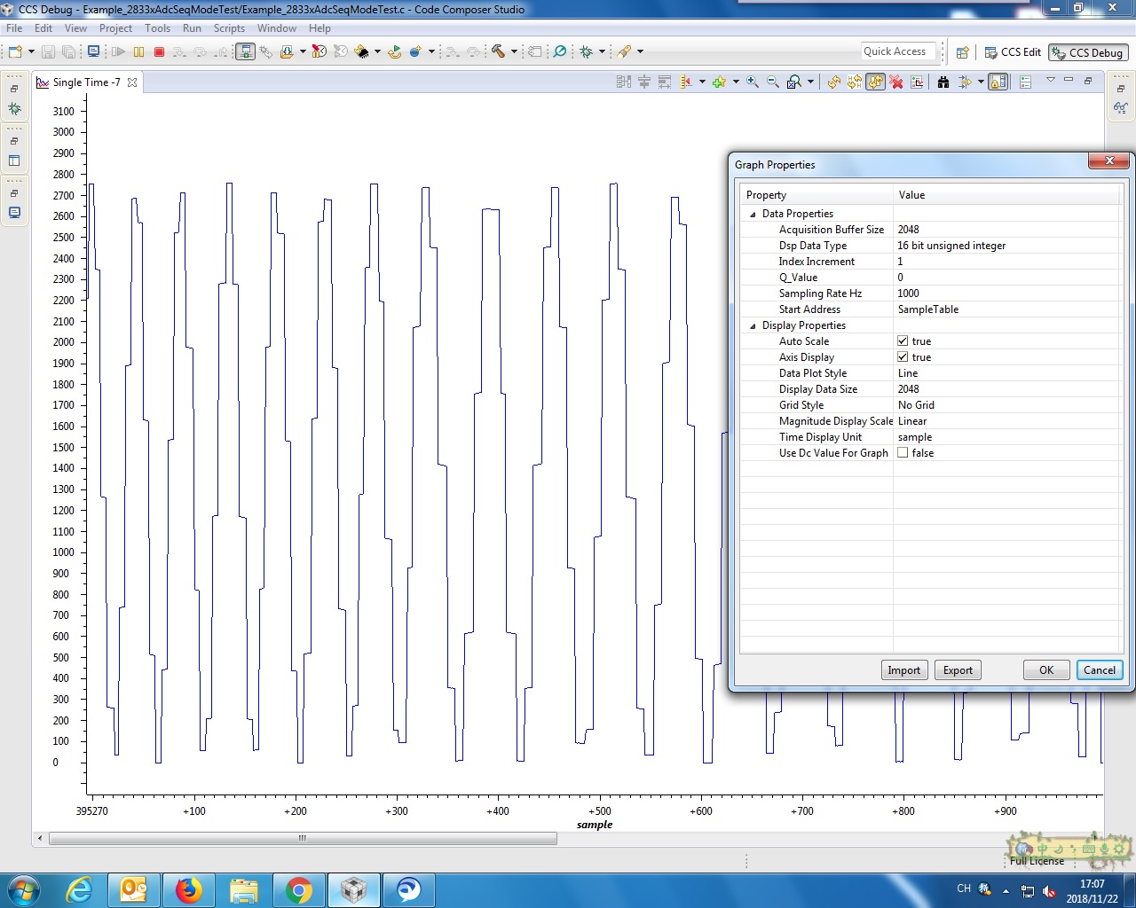
When I gave a 1KHz and 0~2V Sine wave to the ADCINA0 channel, I got a wrong wave in the graph as show below:

Did I make the wrong setting of graph?

Or any other problem?

Best Regards

  • Setting
  • Hi,

    Is your sampling rate 1kHz correct? Can you paste the code?

    Regards,
    Gautam
  • Dear Gautam:

    I use the official example routine at: C:\ti\controlSUITE\device_support\f2833x\v142\DSP2833x_examples_ccsv5\adc_seqmode_test

    Below is the source code:

    #include "DSP28x_Project.h" // Device Headerfile and Examples Include File

    // ADC start parameters
    #if (CPU_FRQ_150MHZ) // Default - 150 MHz SYSCLKOUT
    #define ADC_MODCLK 0x3 // HSPCLK = SYSCLKOUT/2*ADC_MODCLK2 = 150/(2*3) = 25.0 MHz
    #endif
    #if (CPU_FRQ_100MHZ)
    #define ADC_MODCLK 0x2 // HSPCLK = SYSCLKOUT/2*ADC_MODCLK2 = 100/(2*2) = 25.0 MHz
    #endif
    #define ADC_CKPS 0x1 // ADC module clock = HSPCLK/2*ADC_CKPS = 25.0MHz/(1*2) = 12.5MHz
    #define ADC_SHCLK 0xf // S/H width in ADC module periods = 16 ADC clocks
    #define AVG 1000 // Average sample limit
    #define ZOFFSET 0x00 // Average Zero offset
    #define BUF_SIZE 2048 // Sample buffer size

    // Global variable for this example
    Uint16 SampleTable[BUF_SIZE];

    main()
    {
    Uint16 i;

    // Step 1. Initialize System Control:
    // PLL, WatchDog, enable Peripheral Clocks
    // This example function is found in the DSP2833x_SysCtrl.c file.
    InitSysCtrl();

    // Specific clock setting for this example:
    EALLOW;
    SysCtrlRegs.HISPCP.all = ADC_MODCLK; // HSPCLK = SYSCLKOUT/ADC_MODCLK
    EDIS;

    // Step 2. Initialize GPIO:
    // This example function is found in the DSP2833x_Gpio.c file and
    // illustrates how to set the GPIO to it's default state.
    // InitGpio(); // Skipped for this example

    // Step 3. Clear all interrupts and initialize PIE vector table:
    // Disable CPU interrupts
    DINT;

    // Initialize the PIE control registers to their default state.
    // The default state is all PIE interrupts disabled and flags
    // are cleared.
    // This function is found in the DSP2833x_PieCtrl.c file.
    InitPieCtrl();

    // Disable CPU interrupts and clear all CPU interrupt flags:
    IER = 0x0000;
    IFR = 0x0000;

    // Initialize the PIE vector table with pointers to the shell Interrupt
    // Service Routines (ISR).
    // This will populate the entire table, even if the interrupt
    // is not used in this example. This is useful for debug purposes.
    // The shell ISR routines are found in DSP2833x_DefaultIsr.c.
    // This function is found in DSP2833x_PieVect.c.
    InitPieVectTable();

    // Step 4. Initialize all the Device Peripherals:
    // This function is found in DSP2833x_InitPeripherals.c
    // InitPeripherals(); // Not required for this example
    InitAdc(); // For this example, init the ADC

    // Specific ADC setup for this example:
    AdcRegs.ADCTRL1.bit.ACQ_PS = ADC_SHCLK;
    AdcRegs.ADCTRL3.bit.ADCCLKPS = ADC_CKPS;
    AdcRegs.ADCTRL1.bit.SEQ_CASC = 1; // 1 Cascaded mode
    AdcRegs.ADCCHSELSEQ1.bit.CONV00 = 0x0;
    AdcRegs.ADCTRL1.bit.CONT_RUN = 1; // Setup continuous run


    // Step 5. User specific code, enable interrupts:

    // Clear SampleTable
    for (i=0; i<BUF_SIZE; i++)
    {
    SampleTable[i] = 0;
    }

    // Start SEQ1
    AdcRegs.ADCTRL2.all = 0x2000;

    // Take ADC data and log the in SampleTable array
    for(;;)
    {
    for (i=0; i<AVG; i++)
    {
    while (AdcRegs.ADCST.bit.INT_SEQ1== 0) {} // Wait for interrupt
    AdcRegs.ADCST.bit.INT_SEQ1_CLR = 1;
    SampleTable[i] =((AdcRegs.ADCRESULT0>>4) );
    }
    }
    }

  • F.F,

    That appears to work on my setup.  Can you try with a DC signal first to make sure it works as expected?  Then start with a slow frequency (like 2Hz) and see if there's an input frequency where the graph stops working.

    -Tommy

  • Dear Tommy:

    Below is the wave of 2Hz, 100Hz and 1.1KHz. And the 1KHz sine wave is the same as the previous one. I have no idea about those phenomena. Can you give me some reminders?

    1, 2Hz

    2, 100Hz

    3, 1.1KHz

  • Wish for your reply.

    Best Regards

  • F.F,

    It looks as though your device may not be running at the expected frequency.  You can check the ADC sampling rate in the example by toggling a pin like GPIO31, which also happens to control the LD2 LED on the controlCARD.

    Please modify the example with the following:

    Configure GPIO31 to be an output by adding this between the "Clear SampleTable" loop and "Start SEQ1" instruction:

        EALLOW;
        GpioCtrlRegs.GPAMUX2.bit.GPIO31 = 0;  // GPIO31 = GPIO31
        GpioCtrlRegs.GPADIR.bit.GPIO31 = 1;   // GPIO31 = output
        EDIS;

    Then toggle GPIO31 in your ADC sampling loop by adding this after the INT_SEQ1_CLR bit is set:

        GpioDataRegs.GPATOGGLE.bit.GPIO31 = 1;

    You can expect to see a square wave of about 368kHz using an oscilloscope on GPIO31 of the docking station.  The LED should appear to be on.

    -Tommy

  • F.F,

    It has been a while since your last update. I assume that you were able to resolve your issue. If this isn’t the case, please reject this resolution and reply to this thread. If this thread is locked, please make a new thread describing the current status of your issue.

    -Tommy