This thread has been locked.

If you have a related question, please click the "Ask a related question" button in the top right corner. The newly created question will be automatically linked to this question.

LAUNCHXL-F28379D: Customize CMD file cause PC stuck in boot rom on F28379D

Part Number: LAUNCHXL-F28379D

Hi expert,

My application toggles GPIO on F28379D launch pad. The boot switch of launch pad is set to “1”, “1”, “1”. I find I am not able to boot the program from flash on power up using my own CMD file (please see attached).

The program counter is trapped at address 0x3FF16A, which located in Boot memory. Is it related to “Wait Boot Mode”? If I change the CMD file to “2837xD_FLASH_lnk_cpu1.cmd” everything works well.

For “2837xD_FLASH_lnk_cpu1.cmd”, BEGIN is at the front of FLASHA at address 0x080000. But, in SECTIONS part of CMD file, it didn’t even use FLASHA, if there any reason for this? I would like to know what’s wrong with my own CMD file.

BTW, any document describes CMD file in detail?

MEMORY
{
PAGE 0 :  /* Program Memory */
          /* Memory (RAM/FLASH) blocks can be moved to PAGE1 for data allocation */
          /* BEGIN is used for the "boot to Flash" bootloader mode   */

   BEGIN           	: origin = 0x080000, length = 0x000002
   RAMM0           	: origin = 0x000122, length = 0x0002DE
   RAMD0           	: origin = 0x00B000, length = 0x000800
   RAMLS0          	: origin = 0x008000, length = 0x000800
   RAMLS1          	: origin = 0x008800, length = 0x000800
   RAMLS2      		: origin = 0x009000, length = 0x000800
   RAMLS3      		: origin = 0x009800, length = 0x000800
   RAMLS4      		: origin = 0x00A000, length = 0x000800
   RAMGS14          : origin = 0x01A000, length = 0x001000     /* Only Available on F28379D, F28377D, F28375D devices. Remove line on other devices. */
   RAMGS15          : origin = 0x01B000, length = 0x001000     /* Only Available on F28379D, F28377D, F28375D devices. Remove line on other devices. */
   RESET           	: origin = 0x3FFFC0, length = 0x000002

   /* Flash sectors */
   FLASHA           : origin = 0x080002, length = 0x001FFE  /* on-chip Flash */
   FLASHBtoG        : origin = 0x082000, length = 0x01E000	/* on-chip Flash */
   FLASHHtoN        : origin = 0x0A0000, length = 0x020000	/* on-chip Flash */

PAGE 1 : /* Data Memory */
         /* Memory (RAM/FLASH) blocks can be moved to PAGE0 for program allocation */

   BOOT_RSVD       : origin = 0x000002, length = 0x000120     /* Part of M0, BOOT rom will use this for stack */
   RAMM1           : origin = 0x000400, length = 0x000400     /* on-chip RAM block M1 */
   RAMD1           : origin = 0x00B800, length = 0x000800

   RAMLS5      : origin = 0x00A800, length = 0x000800

   RAMGS0      : origin = 0x00C000, length = 0x001000
   RAMGS1      : origin = 0x00D000, length = 0x001000
   RAMGS2      : origin = 0x00E000, length = 0x001000
   RAMGS3      : origin = 0x00F000, length = 0x001000
   RAMGS4      : origin = 0x010000, length = 0x001000
   RAMGS5      : origin = 0x011000, length = 0x001000
   RAMGS6      : origin = 0x012000, length = 0x001000
   RAMGS7      : origin = 0x013000, length = 0x001000
   RAMGS8      : origin = 0x014000, length = 0x001000
   RAMGS9      : origin = 0x015000, length = 0x001000
   RAMGS10     : origin = 0x016000, length = 0x001000
   RAMGS11     : origin = 0x017000, length = 0x001000
   RAMGS12     : origin = 0x018000, length = 0x001000     /* Only Available on F28379D, F28377D, F28375D devices. Remove line on other devices. */
   RAMGS13     : origin = 0x019000, length = 0x001000     /* Only Available on F28379D, F28377D, F28375D devices. Remove line on other devices. */

   CPU2TOCPU1RAM   : origin = 0x03F800, length = 0x000400
   CPU1TOCPU2RAM   : origin = 0x03FC00, length = 0x000400
}

SECTIONS
{
   /* Allocate program areas: */
   .cinit              : > FLASHBtoG      PAGE = 0, ALIGN(4)
   .pinit              : > FLASHBtoG      PAGE = 0, ALIGN(4)
   .text               : > FLASHBtoG      PAGE = 0, ALIGN(4)
   codestart           : > FLASHA         PAGE = 0, ALIGN(4)

   /* Allocate uninitalized data sections: */
   .stack              : > RAMM1        PAGE = 1
   .ebss               : >> RAMLS5 | RAMGS0 | RAMGS1       PAGE = 1
   .esysmem            : > RAMLS5       PAGE = 1
   .cio                : > RAMLS5       PAGE = 1
   
   /* Initalized sections go in Flash */
   .econst             : > FLASHBtoG      PAGE = 0, ALIGN(4)
   .switch             : > FLASHBtoG      PAGE = 0, ALIGN(4)

   .reset              : > RESET,     PAGE = 0, TYPE = DSECT /* not used, */

   Filter_RegsFile     : > RAMGS0,	   PAGE = 1

   SHARERAMGS0		: > RAMGS0,		PAGE = 1
   SHARERAMGS1		: > RAMGS1,		PAGE = 1
   ramgs0           : > RAMGS0,     PAGE = 1
   ramgs1           : > RAMGS1,     PAGE = 1

#ifdef __TI_COMPILER_VERSION__
	#if __TI_COMPILER_VERSION__ >= 15009000
	.TI.ramfunc : {} LOAD = FLASHBtoG,
						 RUN = RAMLS0 | RAMLS1 | RAMLS2 |RAMLS3,
                         LOAD_START(_RamfuncsLoadStart),
                         LOAD_SIZE(_RamfuncsLoadSize),
                         LOAD_END(_RamfuncsLoadEnd),
                         RUN_START(_RamfuncsRunStart),
                         RUN_SIZE(_RamfuncsRunSize),
                         RUN_END(_RamfuncsRunEnd),
						 PAGE = 0, ALIGN(4)
	#else
   ramfuncs            : LOAD = FLASHBtoG,
                         RUN = RAMLS0 | RAMLS1 | RAMLS2 |RAMLS3,
                         LOAD_START(_RamfuncsLoadStart),
                         LOAD_SIZE(_RamfuncsLoadSize),
                         LOAD_END(_RamfuncsLoadEnd),
                         RUN_START(_RamfuncsRunStart),
                         RUN_SIZE(_RamfuncsRunSize),
                         RUN_END(_RamfuncsRunEnd),
                         PAGE = 0, ALIGN(4)
    #endif
#endif

   /* The following section definitions are required when using the IPC API Drivers */
    GROUP : > CPU1TOCPU2RAM, PAGE = 1
    {
        PUTBUFFER
        PUTWRITEIDX
        GETREADIDX
    }

    GROUP : > CPU2TOCPU1RAM, PAGE = 1
    {
        GETBUFFER :    TYPE = DSECT
        GETWRITEIDX :  TYPE = DSECT
        PUTREADIDX :   TYPE = DSECT
    }

   /* The following section definition are for SDFM examples */
   Filter1_RegsFile : > RAMGS1,	PAGE = 1, fill=0x1111
   Filter2_RegsFile : > RAMGS2,	PAGE = 1, fill=0x2222
   Filter3_RegsFile : > RAMGS3,	PAGE = 1, fill=0x3333
   Filter4_RegsFile : > RAMGS4,	PAGE = 1, fill=0x4444
   Difference_RegsFile : >RAMGS5, 	PAGE = 1, fill=0x3333
}

/*
//===========================================================================
// End of file.
//===========================================================================
*/

Thanks

Sheldon

  • I uploaded the wrong one, this CMD is actually getting some problem.

    MEMORY
    {
    PAGE 0 :  /* Program Memory */
              /* Memory (RAM/FLASH) blocks can be moved to PAGE1 for data allocation */
              /* BEGIN is used for the "boot to Flash" bootloader mode   */
    
       BEGIN           	: origin = 0x080000, length = 0x000002
       RAMM0           	: origin = 0x000122, length = 0x0002DE
       RAMD0           	: origin = 0x00B000, length = 0x000800
       RAMLS0          	: origin = 0x008000, length = 0x000800
       RAMLS1          	: origin = 0x008800, length = 0x000800
       RAMLS2      		: origin = 0x009000, length = 0x000800
       RAMLS3      		: origin = 0x009800, length = 0x000800
       RAMLS4      		: origin = 0x00A000, length = 0x000800
       RAMGS14          : origin = 0x01A000, length = 0x001000     /* Only Available on F28379D, F28377D, F28375D devices. Remove line on other devices. */
       RAMGS15          : origin = 0x01B000, length = 0x001000     /* Only Available on F28379D, F28377D, F28375D devices. Remove line on other devices. */
       RESET           	: origin = 0x3FFFC0, length = 0x000002
    
       /* Flash sectors */
       //FLASHA           : origin = 0x080002, length = 0x001FFE  /* on-chip Flash */
       //FLASHBtoG        : origin = 0x082000, length = 0x01E000	/* on-chip Flash */
       FLASHAtoG        : origin = 0x080002, length = 0x01FFFE	/* on-chip Flash */
       FLASHHtoN        : origin = 0x0A0000, length = 0x020000	/* on-chip Flash */
    
    PAGE 1 : /* Data Memory */
             /* Memory (RAM/FLASH) blocks can be moved to PAGE0 for program allocation */
    
       BOOT_RSVD       : origin = 0x000002, length = 0x000120     /* Part of M0, BOOT rom will use this for stack */
       RAMM1           : origin = 0x000400, length = 0x000400     /* on-chip RAM block M1 */
       RAMD1           : origin = 0x00B800, length = 0x000800
    
       RAMLS5      : origin = 0x00A800, length = 0x000800
    
       RAMGS0      : origin = 0x00C000, length = 0x001000
       RAMGS1      : origin = 0x00D000, length = 0x001000
       RAMGS2      : origin = 0x00E000, length = 0x001000
       RAMGS3      : origin = 0x00F000, length = 0x001000
       RAMGS4      : origin = 0x010000, length = 0x001000
       RAMGS5      : origin = 0x011000, length = 0x001000
       RAMGS6      : origin = 0x012000, length = 0x001000
       RAMGS7      : origin = 0x013000, length = 0x001000
       RAMGS8      : origin = 0x014000, length = 0x001000
       RAMGS9      : origin = 0x015000, length = 0x001000
       RAMGS10     : origin = 0x016000, length = 0x001000
       RAMGS11     : origin = 0x017000, length = 0x001000
       RAMGS12     : origin = 0x018000, length = 0x001000     /* Only Available on F28379D, F28377D, F28375D devices. Remove line on other devices. */
       RAMGS13     : origin = 0x019000, length = 0x001000     /* Only Available on F28379D, F28377D, F28375D devices. Remove line on other devices. */
    
       CPU2TOCPU1RAM   : origin = 0x03F800, length = 0x000400
       CPU1TOCPU2RAM   : origin = 0x03FC00, length = 0x000400
    }
    
    SECTIONS
    {
       /* Allocate program areas: */
       .cinit              : > FLASHAtoG      PAGE = 0, ALIGN(4)
       .pinit              : > FLASHAtoG      PAGE = 0, ALIGN(4)
       .text               : > FLASHAtoG      PAGE = 0, ALIGN(4)
       codestart           : > BEGIN         PAGE = 0, ALIGN(4)
    
       /* Allocate uninitalized data sections: */
       .stack              : > RAMM1        PAGE = 1
       .ebss               : >> RAMLS5 | RAMGS0 | RAMGS1       PAGE = 1
       .esysmem            : > RAMLS5       PAGE = 1
       .cio                : > RAMLS5       PAGE = 1
       
       /* Initalized sections go in Flash */
       .econst             : > FLASHAtoG      PAGE = 0, ALIGN(4)
       .switch             : > FLASHAtoG      PAGE = 0, ALIGN(4)
    
       .reset              : > RESET,     PAGE = 0, TYPE = DSECT /* not used, */
    
       Filter_RegsFile     : > RAMGS0,	   PAGE = 1
    
       SHARERAMGS0		: > RAMGS0,		PAGE = 1
       SHARERAMGS1		: > RAMGS1,		PAGE = 1
       ramgs0           : > RAMGS0,     PAGE = 1
       ramgs1           : > RAMGS1,     PAGE = 1
    
    #ifdef __TI_COMPILER_VERSION__
    	#if __TI_COMPILER_VERSION__ >= 15009000
    	.TI.ramfunc : {} LOAD = FLASHAtoG,
    						 RUN = RAMLS0 | RAMLS1 | RAMLS2 |RAMLS3,
                             LOAD_START(_RamfuncsLoadStart),
                             LOAD_SIZE(_RamfuncsLoadSize),
                             LOAD_END(_RamfuncsLoadEnd),
                             RUN_START(_RamfuncsRunStart),
                             RUN_SIZE(_RamfuncsRunSize),
                             RUN_END(_RamfuncsRunEnd),
    						 PAGE = 0, ALIGN(4)
    	#else
       ramfuncs            : LOAD = FLASHAtoG,
                             RUN = RAMLS0 | RAMLS1 | RAMLS2 |RAMLS3,
                             LOAD_START(_RamfuncsLoadStart),
                             LOAD_SIZE(_RamfuncsLoadSize),
                             LOAD_END(_RamfuncsLoadEnd),
                             RUN_START(_RamfuncsRunStart),
                             RUN_SIZE(_RamfuncsRunSize),
                             RUN_END(_RamfuncsRunEnd),
                             PAGE = 0, ALIGN(4)
        #endif
    #endif
    
       /* The following section definitions are required when using the IPC API Drivers */
        GROUP : > CPU1TOCPU2RAM, PAGE = 1
        {
            PUTBUFFER
            PUTWRITEIDX
            GETREADIDX
        }
    
        GROUP : > CPU2TOCPU1RAM, PAGE = 1
        {
            GETBUFFER :    TYPE = DSECT
            GETWRITEIDX :  TYPE = DSECT
            PUTREADIDX :   TYPE = DSECT
        }
    
       /* The following section definition are for SDFM examples */
       Filter1_RegsFile : > RAMGS1,	PAGE = 1, fill=0x1111
       Filter2_RegsFile : > RAMGS2,	PAGE = 1, fill=0x2222
       Filter3_RegsFile : > RAMGS3,	PAGE = 1, fill=0x3333
       Filter4_RegsFile : > RAMGS4,	PAGE = 1, fill=0x4444
       Difference_RegsFile : >RAMGS5, 	PAGE = 1, fill=0x3333
    }
    
    /*
    //===========================================================================
    // End of file.
    //===========================================================================
    */
    

  • in the original file codestart was going to FLASHA. In your modified file you are directing codestart to BEGIN which is at address 0x80000.
    I suppose this is causing the problem. Can you update this and check.

    0x80000 is where the first instruction of your application resides. With your modified cmd file you seem to corrupt that.

    Regards

    Baskaran

  • Baskaran,

    I have move the program to FLASHAtoG which start at 0x080002, after code start branch which reside at 0x080000.

    Sheldon
  • i believe you shouldn't touch 0x80000 to 0x80002. Your code start should go to 0x80002.
  • Hi

    I attached my c file here. In the loop, their is a LB command to jump.

    Please tell me how to change the code to make it right.

    //###########################################################################
    //
    // FILE:    GpioToggle.c
    //
    // TITLE:   GPIO toggle test program.
    //
    //! \addtogroup cpu01_example_list
    //! <h1>GPIO toggle test program (GpioToggle)</h1>
    //!
    //! Three different examples are included. Select the example
    //! (data, set/clear or toggle) to execute before compiling using
    //! the #define statements found at the top of the code.
    //!
    //! Toggle all of the GPIO PORT pins
    //!
    //! The pins can be observed using Oscilloscope.
    //!
    //
    //###########################################################################
    // $TI Release: F2837xD Support Library v3.05.00.00 $
    // $Release Date: Thu Oct 18 15:48:42 CDT 2018 $
    // $Copyright:
    // Copyright (C) 2013-2018 Texas Instruments Incorporated - http://www.ti.com/
    //
    // Redistribution and use in source and binary forms, with or without 
    // modification, are permitted provided that the following conditions 
    // are met:
    // 
    //   Redistributions of source code must retain the above copyright 
    //   notice, this list of conditions and the following disclaimer.
    // 
    //   Redistributions in binary form must reproduce the above copyright
    //   notice, this list of conditions and the following disclaimer in the 
    //   documentation and/or other materials provided with the   
    //   distribution.
    // 
    //   Neither the name of Texas Instruments Incorporated nor the names of
    //   its contributors may be used to endorse or promote products derived
    //   from this software without specific prior written permission.
    // 
    // THIS SOFTWARE IS PROVIDED BY THE COPYRIGHT HOLDERS AND CONTRIBUTORS 
    // "AS IS" AND ANY EXPRESS OR IMPLIED WARRANTIES, INCLUDING, BUT NOT 
    // LIMITED TO, THE IMPLIED WARRANTIES OF MERCHANTABILITY AND FITNESS FOR
    // A PARTICULAR PURPOSE ARE DISCLAIMED. IN NO EVENT SHALL THE COPYRIGHT 
    // OWNER OR CONTRIBUTORS BE LIABLE FOR ANY DIRECT, INDIRECT, INCIDENTAL, 
    // SPECIAL, EXEMPLARY, OR CONSEQUENTIAL DAMAGES (INCLUDING, BUT NOT 
    // LIMITED TO, PROCUREMENT OF SUBSTITUTE GOODS OR SERVICES; LOSS OF USE,
    // DATA, OR PROFITS; OR BUSINESS INTERRUPTION) HOWEVER CAUSED AND ON ANY
    // THEORY OF LIABILITY, WHETHER IN CONTRACT, STRICT LIABILITY, OR TORT 
    // (INCLUDING NEGLIGENCE OR OTHERWISE) ARISING IN ANY WAY OUT OF THE USE 
    // OF THIS SOFTWARE, EVEN IF ADVISED OF THE POSSIBILITY OF SUCH DAMAGE.
    // $
    //###########################################################################
    
    typedef void (* my_function)(void);
    my_function jump2app;
    
    //
    // Included Files
    //
    #include "F28x_Project.h"
    void Gpio_select(void);
    void Gpio_example1(void);
    
    long i = 0;
    
    //
    // Main
    //
    void main(void)
    {
    //
    // Step 1. Initialize System Control:
    // PLL, WatchDog, enable Peripheral Clocks
    // This example function is found in the F2837xD_SysCtrl.c file.
    //
       InitSysCtrl();
    
    //
    // Step 2. Initialize GPIO:
    // This example function is found in the F2837xD_Gpio.c file and
    // illustrates how to set the GPIO to it's default state.
       Gpio_select();
    
    //
    // Step 3. Clear all __interrupts and initialize PIE vector table:
    // Disable CPU __interrupts
    //
       DINT;
    
    //
    // Initialize PIE control registers to their default state.
    // The default state is all PIE __interrupts disabled and flags
    // are cleared.
    // This function is found in the F2837xD_PieCtrl.c file.
    //
       InitPieCtrl();
    
    //
    // Disable CPU __interrupts and clear all CPU __interrupt flags:
    //
       IER = 0x0000;
       IFR = 0x0000;
    
    //
    // Initialize the PIE vector table with pointers to the shell Interrupt
    // Service Routines (ISR).
    // This will populate the entire table, even if the __interrupt
    // is not used in this example.  This is useful for debug purposes.
    // The shell ISR routines are found in F2837xD_DefaultIsr.c.
    // This function is found in F2837xD_PieVect.c.
    //
       InitPieVectTable();
    
    //
    // Step 4. User specific code:
    //
    
        Gpio_example1();
    }
    
    //
    // Gpio_example1 - Example 1: Toggle I/Os using DATA registers
    //
    void Gpio_example1(void)
    {
       for(;;)
       {
          i ++;
          GpioDataRegs.GPBTOGGLE.bit.GPIO34 = 1;
          F28x_usDelay(1000000);
          if(i == 20){
              i = 0;
              asm(" LB 0x080000");
          }
        }
    }
    
    //
    // Gpio_select - Configure GPIO muxing and pin outputs
    //
    void Gpio_select(void)
    {
        EALLOW;
        GpioCtrlRegs.GPAMUX1.all = 0x00000000;  // All GPIO
        GpioCtrlRegs.GPAMUX2.all = 0x00000000;  // All GPIO
        GpioCtrlRegs.GPBMUX1.all = 0x00000000;  // All GPIO
        GpioCtrlRegs.GPADIR.all = 0xFFFFFFFF;   // All outputs
        GpioCtrlRegs.GPBDIR.all = 0x00001FFF;   // All outputs
        EDIS;
    }
    
    //
    // End of file
    //
    

    Thanks

  • Hi Sheldon,

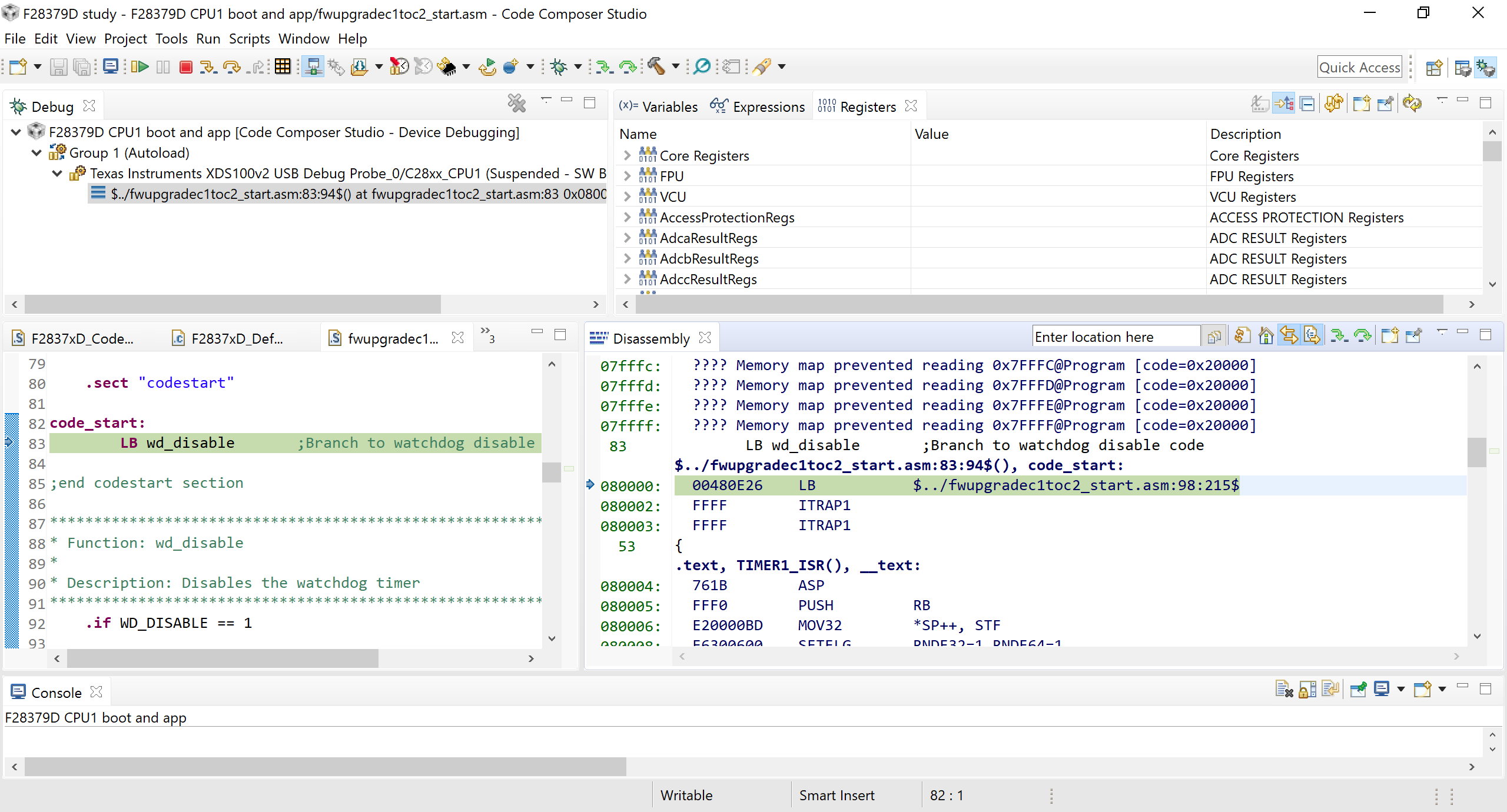
    After loading the application with modified linker command file, what is the assembly instruction at Begin addess (0x080000). you can see this in Disassembly view.

    Regards,
    Sudharsanan
  • Hi Sudharsanan,

    Attached is my screen shoot.

    I have some new finding and the root cause seems behind the CMD file.

    Actually, if I load the PC with some value whose flash content not properly programmed e.g. LB to some blank flash area (without any instruction there). An illegal ISR will trigger. When I POR the device, the main function seems never enter again. If I comment out the LB, POR will be fine.

    Thanks

    Sheldon

  • Sheldon,
    Can you try a quick experiment with below change,
       BEGIN            : origin = 0x080000, length = 0x000010
       FLASHAtoG        : origin = 0x080010, length = 0x01FFE0  /* on-chip Flash */
    Regards
    Baskaran
  • Hi Baskaran,
    I have tried your code sample. Device still will not boot properly.
    Could you try any example code with
    asm(" LB 0x0A0000");
    in main to jump to some "FFFF" area in flash to see if this code can boot successfully from POR?
    I have done the same thing on F28004x, it never seems a problem their. I really want to know the root cause for my customer also met this.

    Sheldon
  • Hi Baskaran,

    Could you reproduce this issue on your side?

    Thanks

    Sheldon

    Attach code for my customer to download

    F28379D boot and app.zip

  • Hi Sheldon,

    Can you please explain the expected flow of the program? In the last message you said 0x80000 was branch address now it has been modified to 0xA0000?

    Can you explain what is the problem seen? and where?

    Regards,
    Sudharsanan
  • Hi Sudharsanan,

    I will update the latest information for you.
    Expected flow: After POR, device boots from flash and entry point is at 0x080000 (this program only use flash sector A). In the main flow, PC will be loaded with some value pointing to some blank flash area (filled with 0xFFFF, such as load PC with 0x0A0000). After this "jump", I hope POR can bring up the device and running this code once again.
    Problem: After I "jump" to some "invalid address". The boot flow seems not successful, the program stuck in some where, maybe in boot rom or in the main function. The blinking LED in main function will not occur.

    Thanks
    Sheldon
  • Hi Sheldon,

    Thanks for the additional information. We tried to recreate the issue here and we understand why the issue is happening.

    1.The CPU GEL file does a CPU Reset hence that should be removed to see the correct behavior of device BootROM. 

    2. The Device_init() code does a disable watchdog(Sysctl_disableWatchdog()) because of which the Watchdog reset did not happen for the CPU to begin the boot process after the application enters illegal ISR. 

    3. We did an explicit Sysctl_enableWatchdog() before branching to the illegal instruction address, which enables the watchdog. and we see the cpu succesfully booting to the application after the issue is created due to watchdog. 

    Hope it helps the customer too to proceed. 

    Regards,

    Sudharsanan 

  • Hi Sudharsanan,

    You are right. I have just tried enable dog before the jump, everything is fine.

    But as for your answers, I still need your help for a better understanding of that.

    Do you mean the "OnReset()" in f2837x.gel will reset the CPU after program load and "re-start"?

    In my understanding, when I run the emulator, it helps me with reset the device correctly which can not be achieved by a POR. Does that mean a POR reset will not rescue me and put me into correct boot rom process from entering an illegal ISR previously but watchdog reset can?

    Thanks

    Sheldon

  • Hi Sheldon,

    If GEL is loaded , on Target Connect, it does a Reset resulting in PC Trapped at BootROM.

    POR is the best way to rescue the system but with the default illegal Operation ISR, the PC is stuck with an ESTOP instruction (with the watchdog disabled). You need some way to bring the system out from that state. This is achieved with Watchdog reset and BootROM executing and entering the Application again.

    Regards,
    Sudharsanan
  • Sheldon,

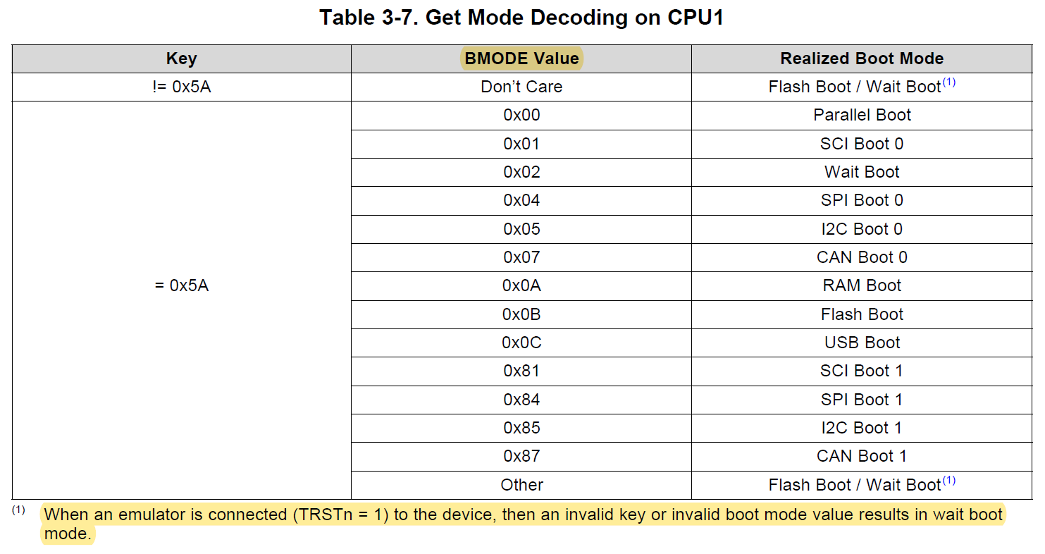
    When emulator (JTAG) is connected, device boots as per the emulation boot (GPIO pin setting are ignored). You need to set correct emulation boot mode to boot the device in such case. If it's not set properly then device will enter into "Wait BOOT" which you are observing. Please refer the TRM for more detail about emulation boot.

    Regards,
    Vivek Singh
  • Hi Vivek and Sudharsanan,

    I tested POR with TRSTn on launch pad pulled low. The boot can be successful. In this case, a watchdog reset is not needed.
    I will refer TRM for more information on wait boot.
    Thanks again for all of you.

    Sheldon
  • Hi Vivek,

    I see below chart in TRM.

    I think either an invalid key or boot mode value cause the device enter wait boot mode when TRSTn = 1. So, I care about will "LB" to some invalid address influence the "key" or "boot mode value"? If so, how does it make it?

    Thanks 

    Sheldon

  • Hi Viviek,

    Do you have any idea on above question?

    Thanks
    Sheldon