This thread has been locked.

If you have a related question, please click the "Ask a related question" button in the top right corner. The newly created question will be automatically linked to this question.

TMS320F28035: TMS320F28035 SPI Data corruption (appears to be clocking 17 bits)

Part Number: TMS320F28035
Other Parts Discussed in Thread: CONTROLSUITE, C2000WARE

Hi,

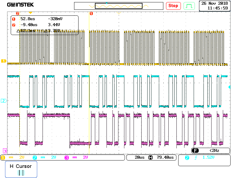
I am experiencing what appears to be a '17' bit transmission on an SPI bus.

I have 8 uCs connected to together and they communicate using the SPI bus (SPI-b) in a daisy chain. uC1 talks to uC2, uC2 talks to uC3 ......uC8 talks back to uC1.

uC1 is the Master.

Data length is 16 Bits (SpibRegs.SPICCR.bit.SPICHAR = 0x1F;)

SPI clock speed is very slow and the scope traces show excellent set up and hold either side of the SPI clock.

The problem:

When i simply route through the Master dummy word, it ripples through perfectly fine and what is received at each uC (and back at the master) is correct.

However, when i then attempt to 'inject' data in the stream (i.e. i 'overwrite what comes in to the uC), the data that gets back to the Master (uC1) is corrupted.

It took a while, but i eventually realised that the data was being shifted 1 bit to the left - suggesting that the uC was clocking 17 bits!

e.g. i inject 8345 (1000-0011-0100-0101) and i get back 068B (0000-0110-1000-1011) - left shifted 1 bit. I have used a number of different data patterns and the result is the same.

I have read the SPI manual from cover to cover a dozen times, i have attempted different speeds (which i dont think it can be as the 'dummy' data runs perfectly fine at all speeds).

I have checked to ensure that there are no spurious edges (the clock 'resting state' is low)

I have checked the 'errata' data, but nothing relevant to the SPI.

Please can anyone help - i am stumped

i include a few code sections associated with SPI set up

SPI_SET_UP

{

EALLOW;

/* Set qualification for selected pins to asynch only */

// This will select asynch (no qualification) for the selected pins.

GpioCtrlRegs.GPAQSEL1.bit.GPIO12 = 3; // Asynch input GPIO12 (SPISIMOB)

GpioCtrlRegs.GPAQSEL1.bit.GPIO13 = 3; // Asynch input GPIO13 (SPISOMIB)

GpioCtrlRegs.GPAQSEL1.bit.GPIO14 = 3; // Asynch input GPIO14 (SPICLKB)

GpioCtrlRegs.GPAQSEL1.bit.GPIO15 = 3; // Asynch input GPIO14 (!SPISTEB)

/* Configure SPI-B pins using GPIO regs*/

// This specifies which of the possible GPIO pins will be SPI functional pins.

GpioCtrlRegs.GPAMUX1.bit.GPIO12 = 3; // Configure GPIO12 as SPISIMOB

GpioCtrlRegs.GPAMUX1.bit.GPIO13 = 3; // Configure GPIO13 as SPISOMIB

GpioCtrlRegs.GPAMUX1.bit.GPIO14 = 3; // Configure GPIO14 as SPICLKB

GpioCtrlRegs.GPAMUX1.bit.GPIO15 = 3; // Configure GPIO115 as SPISTEB

// Enable internal pull-up for the selected pins

// Pull-ups can be enabled or disabled disabled by the user.

// This will enable the pullups for the specified pins.

GpioCtrlRegs.GPAPUD.bit.GPIO12 = 0; //Enable pull-up on GPIO12 (SPISIMOB)

GpioCtrlRegs.GPAPUD.bit.GPIO13 = 0; //Enable pull-up on GPIO13 (SPISOMIB)

GpioCtrlRegs.GPAPUD.bit.GPIO14 = 0; //Enable pull-up on GPIO14 (SPICLKB)

GpioCtrlRegs.GPAPUD.bit.GPIO15 = 0; //Enable pull-up on GPIO15 (SPISTEB)

EDIS;

SpibRegs.SPICCR.all = 0x0F; //Force SPI reset, 16 bit, Clock polarity, loopback off

SpibRegs.SPIBRR = 0x19; //SPI CLOCK speed - slow

SpibRegs.SPICTL.all = 0x02; //CLK_PHASE = 0, Enables Data Transmission, Disable SPI interrupts (poll),// 0 = SLAVE;

SpibRegs.SPICCR.all = 0x8F; //Clear SPI reset

}

My code to tranmsit (Master)

void Read_SPI_Data (void)

{

Receive_Count = 0;

Dummy = 0x0F0F;

SpibRegs.SPITXBUF = Dummy; //Load the Tx buffer with first bytes - Dummy - initiates the clock

while (SpibRegs.SPISTS.bit.INT_FLAG !=1) //While no received character in the buffer - poll the flag

{

Dummy = SpibRegs.SPIRXBUF;                     //clear the flags (read the Rx buffer)

SpibRegs.SPITXBUF = Command_Message; //Load the TxBuffer with the next word = which is COMMAND Word

//Command_Message enables / disables O/Ps and sets overrides etc.

while (SpibRegs.SPISTS.bit.INT_FLAG !=1) //While no received character in the buffer - poll the flag

{ }

Dummy = SpibRegs.SPIRXBUF; //clear the flags (read the Rx buffer)

Dummy = 0x6789; //

while (Receive_Count < 35)                    //Receive_Count is the number of expected words =

{

SpibRegs.SPITXBUF = Dummy;             //Load the TxBuffer with the next word

//Following line checks for Rx flag to be set - indicating that a word has been received by the SPI bus

while (SpibRegs.SPISTS.bit.INT_FLAG !=1) //While no received character in the buffer - poll the flag

{ }

test = SpibRegs.SPIRXBUF; //clear the flags (read the Rx buffer)

SPI_RxArray[Receive_Count] = test; //Put the received data in the RxArray

Receive_Count++; //increment to the next received word

}

Receive_Count = 0; //reset the counter when the Read is complete

test = 0;

}

Slave Read

void Transmit_SPI_Data (void)

{

Receive_Count = 0;

//Following comments apply to the 'first' uC.

//Subsequent uC will similarly receive, but with a gap!

//First received Word is a dummy, which was used to start the transmission

//Second received Word is the COMMAND Word - which is being received when this function is called

while (Receive_Count < 37) //Receive_Count is the number of expected words

{

local_buffer = SpibRegs.SPIRXBUF

local_buffer = 0x8345;       //<This is where i inject the data IF I COMMENT OUT THIS LINE, THE INPUT IS SIMPLY TRANSMITTED OUT AND THERE IS NO CORRUPTION!

SpibRegs.SPITXBUF = local_buffer; //if the data is not for 'this' device - simply route it through


Receive_Count++;

while (SpibRegs.SPISTS.bit.INT_FLAG !=1) //While no received character in the buffer - poll the flag

{ } //This function simply resets the timer

}

//RESET everything!

Receive_Count = 0; //reset the counter

Transmit_Count = 0; //reset the transmit count

}


  • Hello,

    Concerned experts have been notified of this query.

    Note that it is Thanksgiving week in US and most of the TI engineers are away.

    Please expect a delayed response, surely by early next week.


    Regards,

    Sudhakar

    ---------------------------------------------------------------------------------------------------

    If a post answers your question, please mark it with the "verify answer" button.

    Other useful links:

    C2000 Getting Started      C2000 Flash Common Issues/FAQs      Emulation FAQ

  • Hi John.

    I am not quite sure why you are seeing such behavior. If you have the scope traces of the SPI lines, can you send us to get a better understanding. I would like to see SPICLK, SOMI, SIMO and STE(if used) pins

    Regards,
    Veena
  •   Hi Veena,

    I have attached the images you requested

    For clarity I am not using the !SPISTEB signal on the SLAVES, and I have tied them permanently low (I don’t think this would cause the effect I am seeing as this would not affect the SPICLK bit count) and also the dummy data when routed straight through is unaffected. Only when i overwrite does it present the problem.

    The H/W design consists of 8 uC 'daisy chained' together, with uC 1 as the Master. The data stream consists of two 'control' words (each 16 bytes long) followed by dummy data that is overwritten with real data from the following 7 uC (uC2 - uC 8).

    For the purposes of the waveforms, ALL data entering uC2 is overwritten with 8345. However what is coming out is left shifted -068B- (suggesting 17 bit count)

    In image 1, i have attempted to show the set up and hold either side of the SPICLK and show the first 16 bits that are being routed through the uc2.

    Channel 1 is the clock (16 'edges')

    Channel 2 is the data being tranmsitted OUT of uC 2. This data is what should be 8345 , but is left shifted 1 bit and hence 068B.

    Channel 3 is the input to uC2 and is the two control words followd by 'dummy' data (6789 - although i have tried different data patterns)

    In image 2, i am showing the same thing, but over a longer period of time.

    Would appreciate your (or other team members) help in this.

    regards

    J

  • Hi John,

    I will discuss this with my colleagues and get back to you.
    Meanwhile, are you able to see 0x8345 in local_buffer? I hope it did not get left shifted before writing to TXBUF

    Regards,
    Veena
  • Hi Veena,

    Not sure how i can look at the local buffer if what comes out is already shifted?

    Can you advise how i might be able to look at it?

    j

  • Hi John,

    I meant on a debug environment. You can place a breakpoint at the line where the write TXBUF happens and see the contents of local_buffer variable

    Regards,
    Veena
  • Hi Veena,

    Ok i'll give that a go when i get in the office.

    For information i did check to see if there was any way a 'calculation' was being performed (i.e. x2) which might cause a left shift. There is no calculation. The data is simply tranmitted from uC1 to uC2, where it is overwritten.

    J
  • Hi Veena
    I have attempted to use the debugger to monitor the SPITXBUF, SPIRXBUF and the SPIDAT.
    The SPIRXBUF has the correct data in it.
    The SPITXBUF has the correct data in it,
    The SPIDAT has the incorrect data in it i.e. the data is shifted to the left.

    I will admit I am not completely familiar with the subtleties of the debugger, so I may not be using it correctly.

    However, after I allow the debugger to run through a number of lines of code (in the read of the SPIRXBUF loop), the data corrects itself and the data in the SPIDAT register becomes correct. If I then disconnect the debugger (the red button), as I would do when programming the device, the data coming out of the uC is correct (as read on the scope).

    I have refined this process such that if I program the uC, use the ‘run to line’ option to execute the SPITXBUF read, and then disconnect the debugger, the data is correct. This is consistent and suggests that the SPI ‘bit counter’ (which would be 16 for the 16 bits of the SPI character) is now correct. However why the debugger corrects this I don’t know.

    I suspect that there is something anomalous in the SPI set up. Are there any time dependent settings in the SPI set up that need a specific number of clock cycles to complete before allowing data through?

    any suggestions?

    J
  • John,

    A few questions:

    1. Are all of the MCUs on the chain F28035 devices?
    2. If all MCUs are the same device, are they all running the same SW?
    3. While your waveforms captured look great, is there a chance that a spurious noise pulse is coming in to the clock line from MCU2?
    4. Is there any other system event event that seems to cause the corruption? i.e. other code running on the MCU in question?
    5. As a rule, I don't recommend ever tying the Chip select (STE) to 0. I have seen too often where if anything in the system causes a spurious clock pulse, or odd timing issues in the transmissions causes the slaves to lose synchronization with the master. The chip select really is the only way to guard against these types of issues.
    6. Check your SOFT and FREE bits in the SPIPRI register. by default these are set to 0 which means any debug halt will actually halt the SPI. if you have any breakpoints in the code or are debugging MCU 2, there is a chance that you mess with the bit counter in the SPI in undesirable ways. I suggest Setting it to Free Run mode to allow the SPI to always operate.
    7. Generally, with the 8 MCUs, how are you even debugging this? Are you connected to that slave device only? Are you connected to all devices? I am just trying to get a sense of how you are approaching this.
    8. Can you temporarily reduce the number of slaves to just a single master and slave?  It seems like your transmission scheme can handle less slaves without too much work. I have found that reducing the variables is a good way to get to the root of the problem. start cutting things until the problem goes away, then see which step re-introduces the issue.
    9. It does not appear that you are using  FIFO, so this should simplify some things a bit. I do find it difficult to interpret your scope captures without any annotations of what the word should be or where it goes wrong...

    Sorry for the burst of questions, I really don't think that there is any bitshifting going on, it is likely something in how you have architected the SW. If you never see clock bits on the clock line, I don't see a way that this could happen. Forgive me if I am missing anything you may have mentioned earlier.

    Side comment - Please avoid pasting code into the body of the text there is a code formatter tool in the Rich Text Editor  with this icon : </> . you can collapse the code by default. It makes the threads much easier to follow and read as the code is properly formatted. I went ahead and edited your original post to show what that looks like.

  • Of course after I typed all of that up, I am looking harder at your slave Transmit code and see something that could be the culprit. You are immediately reading the SPIRXBUF after entering the the while loop. The first thing in this loop should probably be the poll on the INT_FLAG. Especially without a gate to the SPI transmission and SPI state machine reset provided by the Chip select pin, you could potentially be off by a single bit and never be able to recover.

    Also, I am not sure why you have the Master Read_SPI_Data function using an outer while loop on the INT_Flag. the whole structure of that function seems a bit off. Consider manipulating line 11 to be: while(int_flag !=1) {} //..rest of code..

  • Hi Mark,

    Thanks for coming back to me.

    Answers as follows:

    1 Yes, all are 28035

    2 The Master runs S/W_Master, the 7 slaves run S/W_Slave.

    3 I have gone back to first principles in regards to signal quality. The Clock is very clean (i included a 22R resistor at the transmitting end to improve signal integrity) and the Data is also very clean, As the scope shows the set up and hold time is excellent.

    4 There are no other events occuring in the S/W or the H/W. The design is simply moinitoring a series of voltages using the A/Ds of the Slaves and tranmsitting the result to the Master through the SPI bus. I am using isolated SPI transceivers for each Slave (propogation delay has been measured at <5ns and the signal quality is excellent). There is no heavy current switching which might generate noise. At this time in the testing, i have not connected any of the voltages to be measured and am 'simulating' A/D readings to get the SPI working correctly.

    5 The design includes a repeating 'synchronisation' process that caters for this sort of thing.

    6 Will do

    7 I am presently looking at the output of the first Slave. This receives the Dummy and Control Words (16 btis per Word) from the Master. In the finished application, the Dummy and Control Words are transmitted to the second Slave (then the third....) and the following dummy data is over written with the A/D results. For the purposes of test, i am 'attmepting' to overwrite all the data with 'simluated' A/D data. What is happening is that the simulated data coming out of the first Slave (and the rest) is being corrupted in the way described (shifted LEFT 1 bit). Because all the Slave code is identical (there is a simple 3 bit code read of the H/W to allow the Slave S/W to determine where it is in the sequence and preload a series of data counters), it is proving quite easy.

    8 I could reduce the number of slaves, but this would require cuts and links - which i would rather avoid. As i am able to monitor the o/p of the first Slave, i am effectively redcuing the chain. Also, as mentioned in my earlier submissiion, if i allow the dummy and Control Word to pass through unfettered, the data is not corrupted (which is the weird bit as it suggests i have set everything up correctly).

    9 i did read up on the FIFO useage, but could not see any reason to use this as the deisgn is simple and 'slow'. I will better annotate any future scope traces, unfortunately the scope is not my usual one and i am still learing how to drive it!

    I am looking at the your follow up email regarding the while loop. Will advise later this morning

    Thank you for your support so far

    J

    Re: code submissions - i will use the </> for future code submissions my bad!

  • Hi Mark.

    Well I have a solution of sorts.

    The problem of the SPI bus appearing to clock 17 bits (left shifting by 1 bit) seems to revolve around whether I over write the data coming into the SPI input, or simply allow the data coming in to be transmitted straight out.

    If I do the following:

    Dummy = SpibRegs.SPIRXBUF;

    Dummy = 0xAFAF;                             // overwrite what comes in

    SpibRegs.SPITXBUF = Dummy;

    The data gets corrupted and what comes out of the SPI output is 0x5F5F (left shifted 1 bit)

    If I do the following

    Dummy = SpibRegs.SPIRXBUF;

    SpibRegs.SPITXBUF = Dummy;

    The data comes out of the SPI output un corrupted.

    Clearly I selectively want to overwrite the data coming in so I have introduced a short delay immediately after writing the data.

    Dummy = SpibRegs.SPIRXBUF;

    Dummy = 0xAFAF;                             // overwrite what comes in

    Delay                                                   //delay of a few clock cycles

    SpibRegs.SPITXBUF = Dummy;

    The new data comes out of the SPI output un corrupted.

    It appears that when writing new data destined for the SPI Txbuffer, a few clock cycles are necessary. This is weird – there is nothing in the TI SPI manual suggesting a delay is needed, or any other flags to check.


    It does not seem correct to have to use an arbitrary delay, there must be a register or flag that indicates the new data is ready to transmit.....


    Can you shed any light on this oddity?


    J

  • The INT_FLAG bit is the proper bit to determine if the word is ready to be read or not. Please refer to my previous reply. it seems that you immediately enter the function then write a new value. You need to poll the INT_FLAG before reading SPIRXBUF, then overwrite the value.
  • void Transmit_SPI_Data (void)
    {
        Transmit_Count = 0;
        Receive_Count = 0;
    
        while (Receive_Count < 37)                          //Receive_Count is the number of expected words (37)
        {
            while (SpibRegs.SPISTS.bit.INT_FLAG !=1)        //Wait for the SPI Flag to indicate a new message has arrived - poll the flag!
            {   }
            if ((Receive_Count > (Data_Location - 1)) & (Receive_Count < (Data_Location + 4)))   //simple to determine where to put my SLAVE Data
            {
                Slave_Dummy = SpibRegs.SPIRXBUF;                //Simple read to clear the flags
                Slave_Data = SPI_TxArray[Transmit_Count];		//get the data from the TxArray
                Very_Short_Delay();                             //This short delay is needed !!!!!!!!!!!!
                SpibRegs.SPITXBUF = Slave_Data;             	//Place the data in the TxBuffer
                Transmit_Count++;								//goto the next TxArray location
            }
            else if (Receive_Count == Geographic_Location)      //Identifies the 'COMMAND' Word in the stream  for 'this' location
            {
                Command_Message = SpibRegs.SPIRXBUF;            //Store the 'COMMAND' Word.
               // Very_Short_Delay();
                SpibRegs.SPITXBUF = Command_Message;            //route the COMMAND Word through to the next uC (7 slaves, 1 master)
            }
            else
            {
                Slave_Data = SpibRegs.SPIRXBUF;
               // Very_Short_Delay();
                SpibRegs.SPITXBUF = Slave_Data;      //if the data is not for 'this' device - simply route it through
            }
            Receive_Count++;
        }
        Receive_Count = 0;                                  //reset the counter
        Transmit_Count = 0;                                 //reset the transmit count
    }
    
    
    void SPI_Setup(void)            //SPI Port B
    {
        SpibRegs.SPICCR.bit.SPISWRESET = 0;     	//Force SPI reset
        SpibRegs.SPICCR.bit.SPICHAR = 15;     		//
        SpibRegs.SPICCR.bit.CLKPOLARITY = 0;     	//
        SpibRegs.SPICCR.bit.SPILBK = 0;     		//Force SPI reset, 16 bit, Clock polarity, loopback off
        SpibRegs.SPIBRR = 0x0A;         			//SPI CLOCK speed - slow 0x02
        SpibRegs.SPICTL.all = 0x02;     			//CLK_PHASE = 0, Enables Data Transmission, Disable SPI interrupts (poll),// 0 = SLAVE; (0x0A / 0x02)
        EALLOW;
        // Set qualification for selected pins to asynch only 
        // This will select asynch (no qualification) for the selected pins.
        GpioCtrlRegs.GPAQSEL1.bit.GPIO12 = 3;   // Asynch input GPIO12 (SPISIMOB)
        GpioCtrlRegs.GPAQSEL1.bit.GPIO13 = 3;   // Asynch input GPIO13 (SPISOMIB)
        GpioCtrlRegs.GPAQSEL1.bit.GPIO14 = 3;   // Asynch input GPIO14 (SPICLKB)
        GpioCtrlRegs.GPAQSEL1.bit.GPIO15 = 3;   // Asynch input GPIO14 (!SPISTEB) THIS IS TIED LOW ON THE PCB.
    	// Configure SPI-B pins using GPIO regs
    	// This specifies which of the possible GPIO pins will be SPI functional pins.
        GpioCtrlRegs.GPAMUX1.bit.GPIO12 = 3;    // Configure GPIO12 as SPISIMOB
        GpioCtrlRegs.GPAMUX1.bit.GPIO13 = 3;    // Configure GPIO13 as SPISOMIB
        GpioCtrlRegs.GPAMUX1.bit.GPIO14 = 3;    // Configure GPIO14 as SPICLKB
        GpioCtrlRegs.GPAMUX1.bit.GPIO15 = 3;    // Configure GPIO115 as SPISTEB TIED LOW ON PCB
    	//  GpioCtrlRegs.GPAPUD.bit.GPIO14 = 1;  //Disable pull-up on GPIO14 (SPICLKB).............................................>>>><<<<<
        EDIS;
        SpibRegs.SPICCR.bit.SPISWRESET = 1;     //Clear SPI reset
        GpioDataRegs.GPASET.bit.GPIO6 = 1;      //Enable the SPI Buffer
    }
    
    void Set_Up_Clock(void)
    {
        EALLOW;
            // LOSPCP prescale register settings, normally it will be set to default values
            GpioCtrlRegs.GPAMUX2.bit.GPIO18 = 0;    //Turn off XCLOUT
          //  SysCtrlRegs.LOSPCP.all = 0x0002;        // XCLKOUT to SYSCLKOUT ratio. LSPCLK = SYSCLKOUT / 4
            SysCtrlRegs.LOSPCP.all = 0x0004;      // XCLKOUT to SYSCLKOUT ratio. LSPCLK = SYSCLKOUT / 8
            SysCtrlRegs.XCLK.bit.XCLKOUTDIV = 3;      // Peripheral clock enables set for the selected peripherals. = XCLKOUT 3 = off
            SysCtrlRegs.CLKCTL.bit.XTALOSCOFF = 1;   // Crystal Osc off (internal clock)
            SysCtrlRegs.CLKCTL.bit.XCLKINOFF = 1;   // External Clock input off (internal clock)
            SysCtrlRegs.CLKCTL.bit.INTOSC1OFF = 0;   //  (internal clock)
            SysCtrlRegs.CLKCTL.bit.OSCCLKSRCSEL = 0;    //Internal Osc1 selected OSCCLK
    		
    		//turn off unwanted clocks
            SysCtrlRegs.PCLKCR0.bit.ADCENCLK = 1;      // ADC ----
            SysCtrlRegs.PCLKCR3.bit.COMP1ENCLK = 0;    // COMP1
            SysCtrlRegs.PCLKCR3.bit.COMP2ENCLK = 0;    // COMP2
            SysCtrlRegs.PCLKCR3.bit.COMP3ENCLK = 0;    // COMP3
            SysCtrlRegs.PCLKCR1.bit.ECAP1ENCLK = 0;    // eCAP1
            SysCtrlRegs.PCLKCR0.bit.ECANAENCLK = 0;    // eCAN-A
            SysCtrlRegs.PCLKCR1.bit.EQEP1ENCLK = 0;    // eQEP1
            SysCtrlRegs.PCLKCR1.bit.EPWM1ENCLK = 0;    // ePWM1
            SysCtrlRegs.PCLKCR1.bit.EPWM2ENCLK = 0;    // ePWM2
            SysCtrlRegs.PCLKCR1.bit.EPWM3ENCLK = 0;    // ePWM3
            SysCtrlRegs.PCLKCR1.bit.EPWM4ENCLK = 0;    // ePWM4
            SysCtrlRegs.PCLKCR1.bit.EPWM5ENCLK = 0;    // ePWM5
            SysCtrlRegs.PCLKCR1.bit.EPWM6ENCLK = 0;    // ePWM6
            SysCtrlRegs.PCLKCR1.bit.EPWM7ENCLK = 0;    // ePWM7
            SysCtrlRegs.PCLKCR0.bit.HRPWMENCLK = 0;    // HRPWM
            SysCtrlRegs.PCLKCR0.bit.I2CAENCLK = 0;     // I2C
            SysCtrlRegs.PCLKCR0.bit.LINAENCLK = 0;     // LIN-A
            SysCtrlRegs.PCLKCR3.bit.CLA1ENCLK = 0;     // CLA1
            SysCtrlRegs.PCLKCR0.bit.SCIAENCLK = 0;     // SCI-A
            SysCtrlRegs.PCLKCR0.bit.SPIAENCLK = 0;     // SPI-A
            SysCtrlRegs.PCLKCR0.bit.SPIBENCLK = 1;     // SPI-B -----
            SysCtrlRegs.PCLKCR2.bit.HRCAP1ENCLK = 0;
            SysCtrlRegs.PCLKCR2.bit.HRCAP2ENCLK = 0;
            SysCtrlRegs.PCLKCR0.bit.TBCLKSYNC = 0;     // Enable TBCLK within the ePWM
            EDIS;
    }


    Hi Mark,

    The problem with the SPI bus is still there.

    I agree that polling the INT_FLAG is the correct way of checking to see if the RXBUF is full and ready to be read. My previous code submission did not highlight that I was already doing this, so I have included the code as it stands now.

    You will note that I have included a short delay routine, which prevents the data corruption. However, it should not be necessary as having determined that the RXBUF is full (polling the INT_FLAG), I should be able to simply write any value I like to the TXBUF. If I remove the delay routine, the data is corrupted.

    I don’t believe there is anything wrong with the uC or the structure of the code (everything else works), but I am really at a loss.

    I have also included the set up of the SPI bus procedure and the set up of the clock – thinking that the issue may lie in one of these.

    I really would appreciate any help you can provide

    J

  • This is pretty interesting. the Chip select signal really is the only way to sync /reset the SPI bit counter without resetting the entire module.

    Can you try to introduce some delay on your master transmit. (aka - move your "very_short_delay" to the master and adjust how long the delay needs to be until the issue either resolves or gets worse.
    Can you slow the SPICLK down one value at a time until the problem goes away?
    Alternately, re-introduce the chip select just for debug. does this help as well.

    The INT_FLAG indicates the moment the data from SPIDAT is moved to SPIRXBUF. Based on your SPICLK divider on the master, You should have plenty of SYSCLK cycles to manage this before the next SPICLK occurs. Can you add a GPIO toggle before and after your read and writes to the buffers? show captures with and without the delay. I want to see where in the "dead time" do the buffers get read and written.

    -Mark
  • Hi Mark,

    Thanks for coming back.

    Don’t believe the Chip select pin can be the issue as the problem only occurs when I overwrite what has been received ‘into’ the SLAVE device. If I don’t overwrite (I simply put the received data in the Tx buffer) the data is not corrupted – so the enable pin can have no effect on what ‘I do’ with the received data. Also when I route through data with out overwriting it, it passes through all 7 uC perfectly.

    I have slowed down the master – figuring that there may be a problem of SPICLK speed, but this has had no effect and the very_short_delay was still needed (the delay routine is in the SLAVE – which is counter intuitive). I have tried a number of slower Master speeds and it does not fix the problem. Also, the nature of the corruption suggests that the data is being clocked out one bit earlier (shifted left). This makes me think that the device is left shifting the data that I write to the Tx Buffer. If I were taking too long in the SLAVE to put the data in the TxBuffer, it would be right shifted (i.e.one or more clocks late).

    Introducing the chip select would require a fair bit of ‘cut and link’ (there are 7 Slave and 1 Master uC). I am loathe to do this unless I can clearly see this is the issue and I don’t think it is. I have got good captures of the clock and data and there are clear and distinct clock edges (16 off) and the ‘resting ‘state is low, preventing any spurious edges.

    Good idea with the adding of a GPIO toggle to see where things occur (just hope that doing a bit of GPIO toggling does not cause the problem to go away!). Will give this ago.

    Is there any way we can speed up the correspondence on this issue, as I am under a bit of pressure to progress?


    J

  • John,

    If possible, please send over simplified master and slave code. i know you have copy and pasted both throughout the thread, but just attach the c code. I will see what I can do tomorrow.

    The slave cannot possibly initiate it's own transfer and begin shifting the data early. its just a simple programmable shift register that is clocked by the incoming master clock. I would be curious to see the scope captures of when the slave is receiving the new data and loading it. IF you put the toggle before the read and after the write, it should not affect the timing (alternately just toggle the IO immediately after the write.
    How long is the very short delay anyway?

    -Mark
  • Hi Mark,

    Think I have fixed it!

    The short explanation is that there was a spurious SPICLK edge being generated during the configuration of the MASTER uC. I wrongly assumed that if I do a SPI reset (SPICCR.7 = 0) it would clear the SPI counter and thereby allow me to ‘synch’ all the SLAVES at any time by performing an SPI reset.

    What appears to be happening is that the reset DOES NOT reset the SPI bit count (please confirm this is the case as I cannot find anything that says what ‘will’ reset the bit count), so the data is always 1 bit out (shifted left).

    To fix this, I have now introduced a simple sync process that toggles a signal to the SLAVES and only after receiving the signal is the SLAVE SPI configured. This ‘toggle’ occurs after the MASTER is configured and the clock has settled into its dormant state (low). This prevents a spurious edge (transition from high to low – which is the edge that clocks data into the SLAVES).

    I have read the application note for the umpteenth time, but cannot find anywhere what actually does reset the SPI bit counter. Is it necessary to perform a complete re-configuration of the SPI module to reset the counter?


    J


  • John,

    SPISWRESET will reset the internal bit counter. However, the Master cannot propagate this reset out to the slaves. If they see a single toggle during master config, they cannot know this was spurious. (hence the STE signal being so useful). I will add this clarification to the register description for future improvements.

    I have no problems with your method- keeping the Slaves in reset or disabled until a command is received from the master. Again, this all would be avoided if SPISTE is driven and not tied active.

    SPISWRESET and SPISTE will reset the bit counter. These are the only ways to do so on this device.

    Regards,
    Mark
  • Mark,

    Can you please clarify what is SPISWRESET?

    I agree that the !SPISTE would have been useful to allow the Master to be configured and hold the Slave shift register, but there is nothing anywhere that indicates that it clears the bit counter. Also it seems a little odd that the SPIRESET (SPICCR.7 = 0) does not reset the counter, can i suggest that this is more explicitly described in table 7 of SPRUG71.

    J
  • SPISWRESET is SPICCR.7. I am actually not sure where you are getting "SPIRESET" from all of our documentation that I have is showing SPICCR.7 as SPISWRESET. What version of SPRUG71 are you referring to? How about controlSUITE or C2000Ware versions? if you grab the latest, it is all saying SPISWRESET.

    Agreed that the documentation is lacking. I have already mentioned that I will be adding the clarifications where necessary.

    -Mark