This thread has been locked.

If you have a related question, please click the "Ask a related question" button in the top right corner. The newly created question will be automatically linked to this question.

TMS320F280049: Wrong ADC offset

Part Number: TMS320F280049
Other Parts Discussed in Thread: TIDM-HV-1PH-DCAC

Hi experts,

I am working on a project based on TIDM-HV-1PH-DCAC.

To sample the output voltage, I configured ADC following the example code:

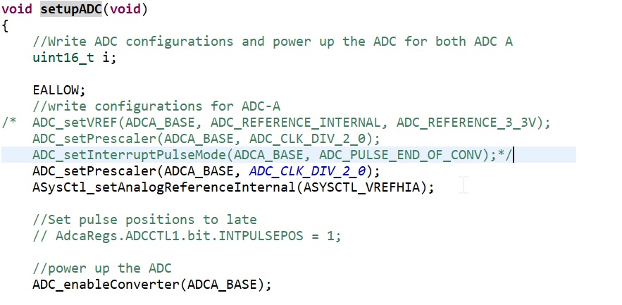
Under this configuration, I believe I am using an internal reference which is 3.3V.

In our sampling circuit, we have a 1.65V offset. So, if the output voltage is 0, I should be able to see a ADC result which is 2048.

However, the sampling result offset is always 1024. 

If the reference is configured to be 2.5, I believe I should have a result of 2703.

Why I am always getting 1024? Where should I try to find the mistake?

BTW: The offset in PPB is 0.

Thanks!

  • I also observed the ADC result of input voltage.
    The result is 0.5 also times of the designed value.
  • Hi Weiqi,

    Is there still an outstanding question? Your input voltage is 1/2 the expected value and the ADC conversion result is correspondingly 1/2 the expected value?

    You can verify that the ADC is in internal reference mode by confirming that the VREFHI pin has an output voltage. If the voltage is 1.65V, the ADC input range is 0 to 3.3V. If the voltage is 2.5V, the ADC input range is 0 to 2.5V.
  • Hi Devin,

    I believe I found reason of this problem.

    On customer’s board, the VrefHI pin is connected to 3.3V. According to the TRM, the VrefHI should be 1.65V if internal 3.3V reference is selected, is that correct? 

    I noticed that on our launchpad the VREFHI is connected to GND with a capacitor, rather than 3.3V. Does the connection with 3.3V cause the wrong state?

    In other word, if internal reference is selected, the VREFHI must be connected to GND with a capacitor?

    Thanks for your reply.

  • Hi Weiqi,

    If the ADC is in internal reference mode, no voltage should be driven onto the pin (including 3.3V VDDA) because the device will drive a voltage out of the pin (to be stabilized by the external capacitance) . Contention between the external voltage and internal voltage will cause operational issues (even in the case that both voltages are nominally the same value).