This thread has been locked.

If you have a related question, please click the "Ask a related question" button in the top right corner. The newly created question will be automatically linked to this question.

TMS320F2808: TMS320F2808 is in reset state, 83pinGPIO24) level problem

Part Number: TMS320F2808

Hello:

The problem is described as follows:

DSP2808 83 pin (GPIO24), 3K resistance pull-down, and power on 200ms of DSP reset time, 83 pin outputs a square wave signal, as shown in the figure:

Different control panel DSP output level is not the same, some DSP output level below 0.5v, some output more than 3V, hardware, software version is the same;

Question: 1. Why there is such a big difference in the high level of DSP pin in the reset state;

2. What is the internal structure of GPIO24? Is it equivalent to pulling up a resistance?
Best Regards

Leon

文晔集团

广东省深圳市南山区高新中三道9号环球数码大厦12

Mobile:(86)159 8985 2994

Tel:(86)755-26743880  Ext:6643

Fax:(86)755-26743990

  • Leon,

                Please refer to section 6.8 of the datasheet (page 106 of SPRS230N):


    "No requirements are placed on the power up/down sequence of the various power pins to ensure the correct reset state for all the modules. However, if the 3.3-V transistors in the level shifting output buffers of the I/O pins are powered prior to the 1.8-V transistors, it is possible for the output buffers to turn on, causing a glitch to occur on the pin during power up. To avoid this behavior, power the VDD (core voltage) pins prior to or simultaneously with the VDDIO (input/output voltage) pins, ensuring that the VDD pins have reached 0.7 V before the VDDIO pins reach 0.7 V".


    I think what you are seeing is the glitch mentioned there. Since it is a glitch, its characteristics are not well-defined and could indeed vary from device to device. Can you confirm if the highlighted requirement is being met in the design? Please capture a scope waveform that clearly shows the timing relationship between 1.8v, 3.3v, -XRS & GPIO24.


    As stated in the datasheet, there is an internal pull-up on all GPIO pins.

  • Hi, Hareesh

    Thank you for your support.


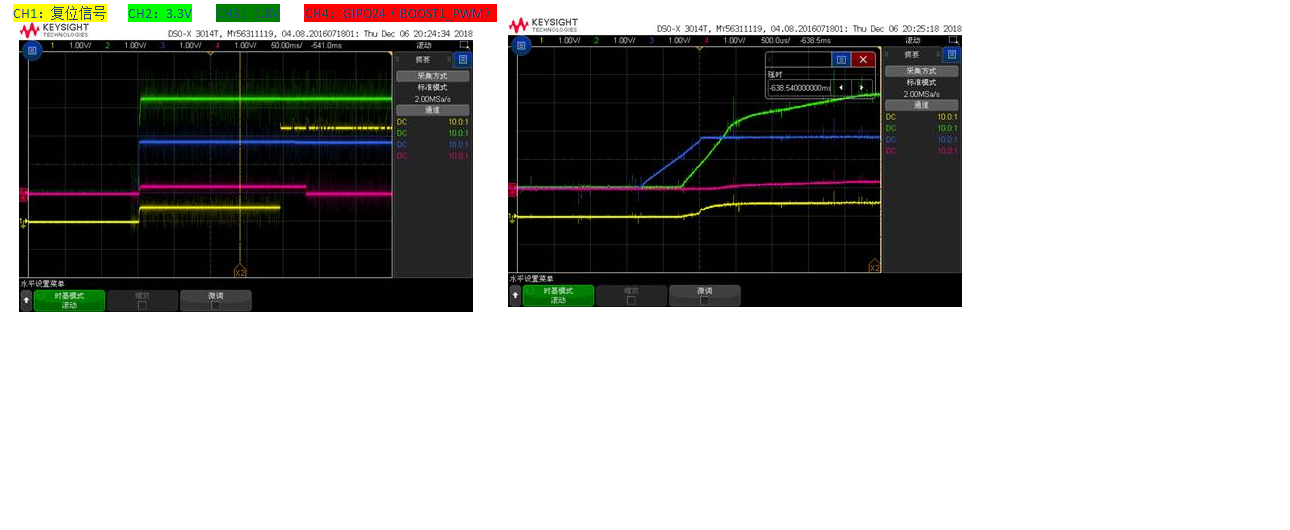
    The waveform is shown as the pic below.

    1.8v is a little faster than 3.3v, that is ok.

    After power on, we will keep the DSP  reset for 200ms, the influence of power on time sequence can be ignored.

    During the reset period, the GPIO24 port outputs a square wave.

    Square wave is comprehensible. Our problem is:

    1. the 3K resistance is pulled down, some control panel output square wave whose amplitude is 0.5v, while some control panel output square wave whose amplitude is  3V (that is a risk),

    what is the reason?

    1. when restoring the output square wave, what is the internal state of GPIO24? Is it equivalent to a pulled up resistance and what is the value of the resistance?

  • Leon,
    Basically, you are saying that even though the power-sequencing guideline is being met (by virtue of 1.8v ramping ahead of 3.3v), the glitch is still seen. Is this correct?

    The internal pull-up is not a physical resistor. It is an "active circuit".

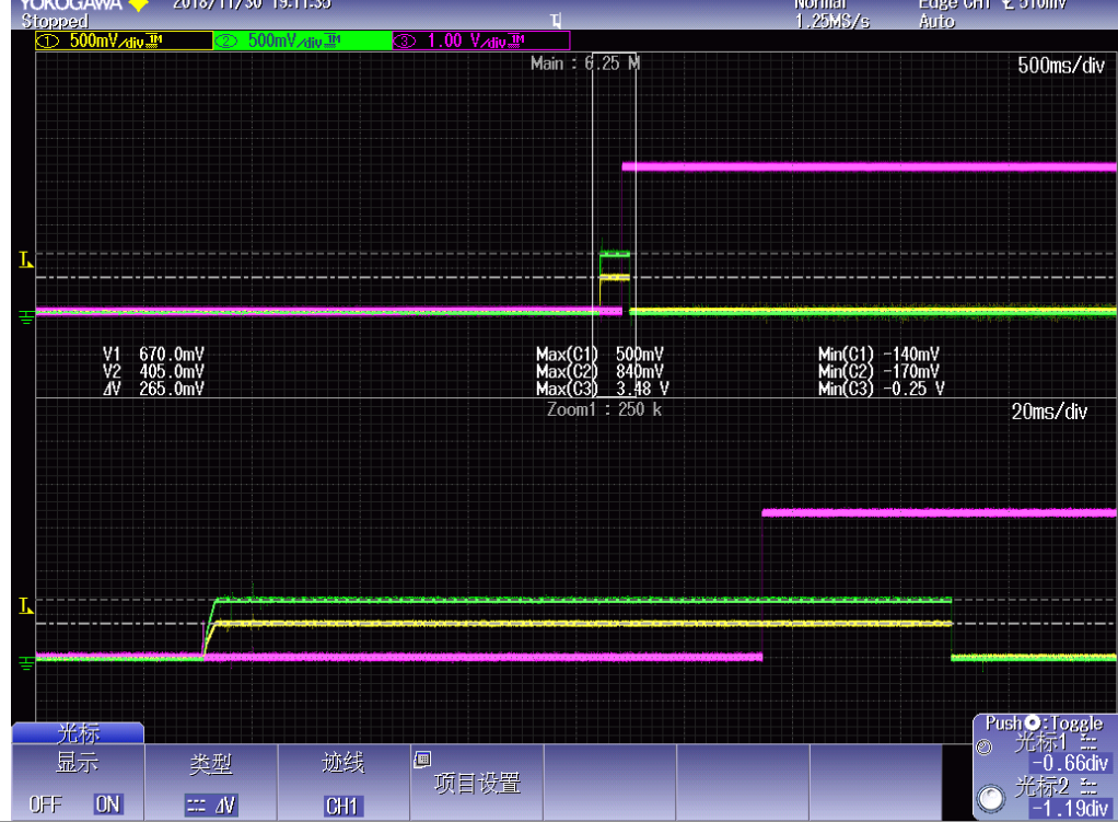
    The next time you send the scope captures, please separate the channels so that it is easy to discern which color is which channel. Also, channel 1 is marked in Chinese. Is this -XRS? If so, why does it appear to be pulsing randomly?
  • Could you please share the circuit that is driving the –XRS pin and also the circuitry connected to GPIO24 pin?

    Why isn’t –XRS low completely when it is active? It appears to raise to 500 mV for a while and then raise to 3.3v. Also, I see a lot of noise on all 4 channels. The next time you send a scope image, please send a high-resolution image. The ones you sent is very hard analyze.

    Does the circuit use a crystal or an external oscillator? Could you please send a scope capture that captures the following: Clock i/p to the device, 1.8v, 3.3v, XRS pin?
  • I haven’t heard from you for a while. I presume you have been able to resolve the issue. If this is not the case, please respond to my questions in my last 2 posts.