Tool/software: Code Composer Studio
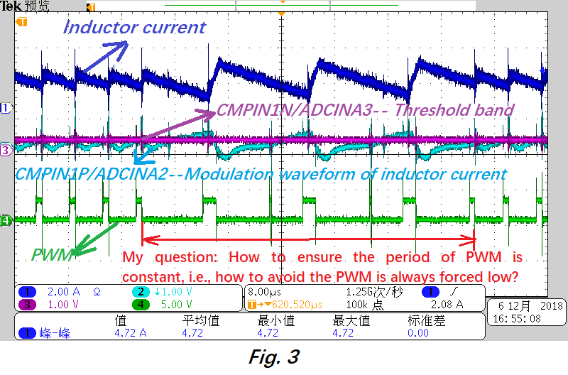
I want to use the CMPSS to realize the peak current mode control of buck converter. Therefore, I write some code to test the CMPSS and ePWM. The test waveforms are as follows, where the light-blue line represents the signal connected in CMPIN1P/ADCINA2 and the pink line represents the signal connected in CMPIN1N/ADCINA3. The green line is the output signal (ePWM6A).

In the code, I set the default duty cycle is 50%, and it is forced to low when the CMPSS trip event occurs. Fig 1 gives the waveforms that the CMPSS is worked and it can force PWM to low. However, according to Fig. 2, when CMPIN1P > CMPIN1N, ePWM is always low, this is not that I want. I hope during the period that CMPIN1P > CMPIN1N, the PWM always has output the duty cycle that I set (50% and not always low). The code are listed as follows, how should I set the registers? Thank you very much!
void InitEPwm6Example(void)
{
    EPwm6Regs.TBPRD = 500;                       // Set timer period
    EPwm6Regs.TBPHS.bit.TBPHS = 0x0000;           // Phase is 0
    EPwm6Regs.TBCTR = 0x0000;                     // Clear counter
    //
    // Setup TBCLK
    //
    EPwm6Regs.TBCTL.bit.CTRMODE = TB_COUNT_UP; // Count up
    EPwm6Regs.TBCTL.bit.PHSEN = TB_DISABLE;        // Disable phase loading
    EPwm6Regs.TBCTL.bit.HSPCLKDIV = TB_DIV1;       // Clock ratio to SYSCLKOUT
    EPwm6Regs.TBCTL.bit.CLKDIV = TB_DIV1;          // Slow just to observe on
    // the scope.
    EPwm6Regs.TBCTL.bit.PHSEN = TB_ENABLE;         //禁止相位控制
    EPwm6Regs.TBCTL.bit.PRDLD = TB_SHADOW;          //TBPRD寄存器采用映射模式
    EPwm6Regs.TBCTL.bit.SYNCOSEL = TB_SYNC_IN; //禁止同步信号
    // Setup compare
    //
    EPwm6Regs.CMPA.bit.CMPA = 250;                   //计数到此,强制拉低
    //
    // Set actions
    //
    EPwm6Regs.AQCTLA.bit.ZRO = AQ_SET;               //在计数为0处,设置EPWMA为高电平
    EPwm6Regs.AQCTLA.bit.CAU = AQ_CLEAR;             // 达到设定计数值CMPA处,EPWMA为低电平
    ///----------------------------------------------------------------------------
    EALLOW;
    //Configure DCB to be TRIP4
    EPwm6Regs.DCTRIPSEL.bit.DCBHCOMPSEL = 3;         //选择Zone4 作为触发Trip 4
    EPwm6Regs.TZDCSEL.bit.DCBEVT2 = TZ_DCBH_HI;      //Digital compare output B event 2 选择
    EPwm6Regs.TZSEL.bit.DCBEVT2 = 1;//Configure DCB as CBC
    //Configure DCB path to be filtered & async
    EPwm6Regs.DCBCTL.bit.EVT2SRCSEL = DC_EVT_FLT;            // Source is DCBEVT2 Signa
    EPwm6Regs.DCBCTL.bit.EVT2FRCSYNCSEL = DC_EVT_SYNC;    // 0: Source Is Synchronous Signal
   //空窗设置
    EPwm6Regs.DCFCTL.bit.BLANKE=1;                        //1: Blanking window is enabled
    EPwm6Regs.DCFCTL.bit.PULSESEL=2;                      // Time-base counter equal to zero (TBCTR = 0x00)
    EPwm6Regs.DCFCTL.bit.SRCSEL=3;                        // Source Is DCBEVT2 Signal
    EPwm6Regs.DCFOFFSET=0;                                //Blanking Window Offset
    EPwm6Regs.DCFWINDOW=30;                               //0.1 us  20


    EPwmXbarRegs.TRIP4MUXENABLE.bit.MUX0 = 1;  //Enable TRIP4 Mux for Output
    EPwm6Regs.TZCTL.bit.TZA=TZ_FORCE_LO;       // Force EPWMxA to a low state
    EPwm6Regs.TZCLR.bit.CBCPULSE=0;            //CTR = zero pulse clears CBC trip latch. (Same as legacy designs.)
    EPwmXbarRegs.TRIP5MUXENABLE.bit.MUX0 = 1;  //Enable TRIP4 Mux for Output
    EDIS;


}

void InitCMPSS(void)
{
    EALLOW;
    //
    //Enable CMPSS
    //
    Cmpss1Regs.COMPCTL.bit.COMPDACE = 1;
    //
    //NEG signal comes from DAC
    //
    Cmpss1Regs.COMPCTL.bit.COMPHSOURCE = NEGIN_PIN;
    //
    //Use VDDA as the reference for DAC
    //
    Cmpss1Regs.COMPDACCTL.bit.SELREF = REFERENCE_VDDA;
    //
    //Set DAC to midpoint for arbitrary reference
    //
//    Cmpss1Regs.DACHVALS.bit.DACVAL = 800;
    //
    // Configure CTRIPOUT path
    // Asynch output feeds CTRIPH and CTRIPOUTH
    //
//    Cmpss1Regs.COMPCTL.bit.CTRIPHSEL = CTRIP_SYNCH;
//    Cmpss1Regs.COMPCTL.bit.CTRIPOUTHSEL = CTRIP_SYNCH;
    EDIS;
}