This thread has been locked.

If you have a related question, please click the "Ask a related question" button in the top right corner. The newly created question will be automatically linked to this question.

TMS320F28377S: ADC accuracy improving solution

Part Number: TMS320F28377S
Other Parts Discussed in Thread: TINA-TI

Hi,

Customer is using F28377S for motor control. High speed 12-bit ADC with over sampling is used to improve the accuracy.

To achieve a better accuracy, some doubts are still there:

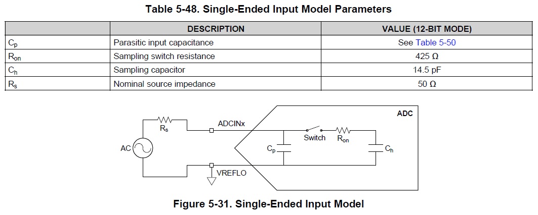
1) Is Ron a fixed value resistance, 425 Ohm?

2) When is the right point for Ch completely charged and discharged?

3) How to select the R and C for the external ADC pins?

4) Do we have the TINA-TI module for ADC?

Their application on ADC is:

1) Monitor BLDC phase current, with 28~36Hz frequency. Low speed motor.

2) Current external ADC pin R is 100 Ohm, with 1 nF C.

3) 1MHz sample frequency.

4) 300ns sampling time.

5) Offset error are calculated, but not gain error.

Thanks a lot.

Br, Jordan

  • Hi Jordan,

    1) Yes this is a fixed resistance for the sake of the model.  425 ohms is a worst case; the observed value on a typical device under ambient conditions will be lower.  

    2) This kinda depends on how much error the application can tolerate.  Quantization error is about 1/2 LSBs and internal ADC noise is around 1 LSBs.  1/4 LSBs will be well below everything, 1/2 LSBs probably won't be noticeable, and 1 LSBs is about on par with other expected errors.  Of course if the system can tolerate more error, allowing for more settling error is fine.  Just keep in mind that settling error will usually not be random, so you can't count on it to be averaged out via oversampling or via multiple iterations of the control loop.  

    3) This is a complicated topic, but briefly:

    Fast sample rate (1Msps would qualify): Cs = 20*Ch, Rs = small (10-100 ohms), drive with an op amp with high BW, S+H = a little higher than minimum

    Slow sample rate: Cs = (2^N)*2*Ch, Rs = potentially large (need to sample slower for larger R), probably no op-amp.  

    4)Nothing official, but you can grab some of the models here:

    You should be able to solve for the worst-case settling error with the customer's current circuit using the following formulas (use the customer's component values and the model values for F28379D).  Note that sample rate shouldn't matter in this case as long as the ADC time + S&H time does not exceed the time between triggers.  This doesn't take into account driving op-amp BW, but BW will need to be roughly > 1 MHz or so.  I can link you some very in depth resources from the SAR ADC + Precision op-amp groups if you want to simulate everything, including the op-amp.  

  • Devin,
    Thanks a lot for your reply.

    1) What about "2) When is the right point for Ch completely charged and discharged?"?
    2) In customer's design, there are some issues:
    - There's the possibility that a negative voltage (-0.2V) could be applied to ADC pins.
    - ADC pin input signal could be over the Vref, which is 3.3V. They even would like to set a Vref higher than Vdda.
    What will happen? Before re-design, customer would like to know some details of our ADC design side.
    Thanks a again.
    Br, Jordan
  • Devin,
    Some more info about "Vref is higher than Vdda". The Vref is fixed with 3.3V, from our Ref3033. Vdda comes from LDO (like 1117). 5V inputs and 3.3V outputs. But, actually it's a little less than 3.3V, like 3.27V. So Vref (3.3V) is higher than Vdda (3.27V).
    What will happen on this issue?
    Thanks a lot.
    Br, Jordan
  • Hi Jordan,

    For 1) I listed the various considerations for what level to consider as 'charged'. The charging starts at the beginning of the S+H period and ends right before the end of the S+H window. Consult the timing diagrams in the datasheet. Does that answer your question?

    The VREFHI should not be larger than VDDA at any point. In your example you might expect minor performance degradation in the ADC. This is why typically you'd use a 2.5V or 3.0V reference for this ADC and not 3.3V (or higher).

    As far as inputs, if the input is above or below the VREF range the ADC output will saturate to the max or min digital value. If the input is high enough above VDDA or low enough below VSSA (figure above or below 0.3V to be safe) the protection diodes inside the ADC input will begin conducting (and this will cause the voltage to clamp). If the series resistance on the pin(s) doesn't limit the total clamping current to below the datasheet specification (I believe 20mA total, but check the official source) the device may be permanently damaged.
  • Devin,
    Thanks for your explanation.
    We all know that "The VREFHI should not be larger than VDDA at any point". What's the inside logic for VrefHi and Vdda? If VrefHi>Vdda happens, what will the issue be? Something damaged?

    Thanks again.
    Br, Jordan
  • Hi Jordan,

    VREFHI > VDDA will cause incorrect ADC operation.

    VREFHI > VDDA + 0.3V will potentially cause damage.  

  • Devin,
    Thanks for your info. Actually, customer want to know more about these two, as they can happen in their application. Customer would like to have a deep evaluation/analysis, if to call back the products.
    In their application, VrefHi can be a little higher than Vdda, like 0.1V.
    VREFHI > VDDA will cause incorrect ADC operation.
    VREFHI > VDDA + 0.3V will potentially cause damage.

    Thanks a lot.
    Br, Jordan
  • Hi Jordan,

    VREFHI > VDDA will cause the device to operate outside of the datasheet operating conditions:

    We don't know how the device will perform in these conditions.  

    VREFHI > VDDA + 0.3V would potentially be a high enough voltage to turn on internal device clamping diodes.  Since the VREFHI needs to be driven by a low-impedance source, this will likely result in the 20mA clamping current specification being immediately exceeded, causing permanent damage to the device.  Unlike an ADC input, you can't add any external series resistance to the VREFHI pin to limit the potential clamping current.