Part Number: TMS320F28377S
Tool/software: Code Composer Studio
Hi,
I want to synchronize the PWM between board to board.
My program is as below.
void main(void)
{
DINT;
IER = 0x0000;
IFR = 0x0000;
InitSysCtrl();
InitGpio();
Init_LED();
InitEPwm1Gpio();
InitEPwm2Gpio();
InitEPwm3Gpio();
EALLOW;
// GPIO_SetupPinMux(6, GPIO_MUX_CPU1, 3); //Master Board Setting
// GPIO_SetupPinOptions(6, GPIO_OUTPUT, GPIO_PUSHPULL); //Master Board Setting
GPIO_SetupPinMux(7, GPIO_MUX_CPU1, 0); //Slave Board Setting
GPIO_SetupPinOptions(7, GPIO_INPUT, GPIO_ASYNC); //Slave Board Setting
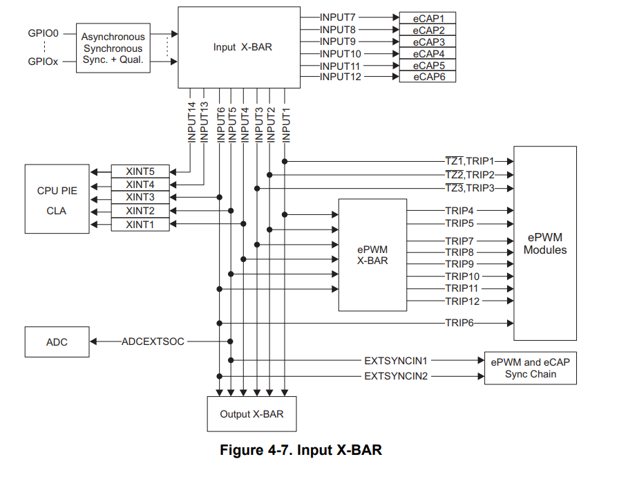
InputXbarRegs.INPUT5SELECT = 7; //Slave Board Setting
EDIS;
InitPieCtrl();
InitPieVectTable();
EALLOW;
PieVectTable.EPWM1_INT = &EPwm1Isr; // Interrupt Service Routine Re-mapping
EDIS;
PieCtrlRegs.PIEIER3.bit.INTx1 = 1; // Enable PIE group 3 interrupt 1 for EPWM4_INT
IER |= M_INT3; // Enable CPU INT3 for EPWM1_INT
EALLOW;
CpuSysRegs.PCLKCR0.bit.TBCLKSYNC = 0;
EDIS;
EALLOW;
ClkCfgRegs.PERCLKDIVSEL.bit.EPWMCLKDIV = 1; // 0: EPWMCLK = SYSCLKOUT = 200MHz
// 1: EPWMCLK = SYSCLKOUT/2 = 100MHz (Default)
EDIS;
InitEPwmModules(); // Initialize EPWM1,2,3 Modules
EALLOW;
CpuSysRegs.PCLKCR0.bit.TBCLKSYNC = 1;
EDIS;
sci_debug_init();
ERTM; /* Enable Global realtime interrupt DBGM */
EINT; /* Enable Global interrupt INTM */
for(;;)
{
BackTicker++;
}
}
interrupt void EPwm1Isr(void)
{
EPwm1Regs.CMPA.bit.CMPA = EPwm1Regs.TBPRD - (EPwm1Regs.TBPRD * 0.5);
EPwm2Regs.CMPA.bit.CMPA = EPwm2Regs.TBPRD - (EPwm2Regs.TBPRD * 0.5);
EPwm3Regs.CMPA.bit.CMPA = EPwm3Regs.TBPRD - (EPwm3Regs.TBPRD * 0.5);
// Clear INT flag for this timer
EPwm1Regs.ETCLR.bit.INT = 1;
// Acknowledge this interrupt to receive more interrupts from group 3
PieCtrlRegs.PIEACK.bit.ACK3 = 1;
}
void InitEPwmModules(void)
{
// Setup TBCLK
EPwm1Regs.TBPRD = (TBCLK/PWMCARRIER)/2; // Set Timer Period
EPwm1Regs.TBCTR = 0; // Clear Counter
EPwm2Regs.TBPRD = (TBCLK/PWMCARRIER)/2; // Set Timer Period
EPwm2Regs.TBCTR = 0; // Clear Counter
EPwm3Regs.TBPRD = (TBCLK/PWMCARRIER)/2; // Set Timer Period
EPwm3Regs.TBCTR = 0; // Clear Counter
// Set Compare values
EPwm1Regs.CMPA.bit.CMPA = 0; // Set Compare A value to 0%
EPwm2Regs.CMPA.bit.CMPA = 0; // Set Compare A value to 0%
EPwm3Regs.CMPA.bit.CMPA = 0; // Set Compare A value to 0%
// Setup counter mode
EPwm1Regs.TBCTL.bit.CTRMODE = 2; // Count Up/Down (Symmetric)
EPwm1Regs.TBPHS.bit.TBPHS = 0; // Phase is 0
EPwm1Regs.TBCTL.bit.PHSEN = 1; // Disable phase loading
EPwm1Regs.TBCTL.bit.SYNCOSEL = 0; // Slave Board Setting
// EPwm1Regs.TBCTL.bit.SYNCOSEL = 1; // Master Board Setting
EPwm1Regs.TBCTL.bit.PRDLD = 0; // Period Register is loaded from its shadow when CNTR=Zero
EPwm1Regs.TBCTL.bit.HSPCLKDIV = 0; // Clock ratio to SYSCLKOUT
EPwm1Regs.TBCTL.bit.CLKDIV = 0; // TBCLK = (SYSCLK / EPWMCLKDIV) / (HSPCLKDIV * CLKDIV)
EPwm2Regs.TBCTL.bit.CTRMODE = 2; // Count Up/Down (Symmetric)
EPwm2Regs.TBPHS.bit.TBPHS = 0; // Phase is 0
EPwm2Regs.TBCTL.bit.PHSEN = 1; // Disable phase loading
EPwm2Regs.TBCTL.bit.SYNCOSEL = 0; // Sync down-stream module
EPwm2Regs.TBCTL.bit.PRDLD = 0; // Period Register is loaded from its shadow when CNTR=Zero
EPwm2Regs.TBCTL.bit.HSPCLKDIV = 0; // Clock ratio to SYSCLKOUT
EPwm2Regs.TBCTL.bit.CLKDIV = 0; // TBCLK = (SYSCLK / EPWMCLKDIV) / (HSPCLKDIV * CLKDIV)
EPwm3Regs.TBCTL.bit.CTRMODE = 2; // Count Up/Down (Symmetric)
EPwm3Regs.TBPHS.bit.TBPHS = 0; // Phase is 0
EPwm3Regs.TBCTL.bit.PHSEN = 1; // Disable phase loading
EPwm3Regs.TBCTL.bit.SYNCOSEL = 0; // Sync down-stream module
EPwm3Regs.TBCTL.bit.PRDLD = 0; // Period Register is loaded from its shadow when CNTR=Zero
EPwm3Regs.TBCTL.bit.HSPCLKDIV = 0; // Clock ratio to SYSCLKOUT
EPwm3Regs.TBCTL.bit.CLKDIV = 0; // TBCLK = (SYSCLK / EPWMCLKDIV) / (HSPCLKDIV * CLKDIV)
// Setup shadowing
EPwm1Regs.CMPCTL.bit.SHDWAMODE = 0; // Enable Shadowing
EPwm1Regs.CMPCTL.bit.LOADAMODE = 0; // Load on CNTR=Zero
EPwm1Regs.CMPCTL.bit.SHDWBMODE = 0; // Enable Shadowing
EPwm1Regs.CMPCTL.bit.LOADBMODE = 0; // Load on CNTR=Zero
EPwm2Regs.CMPCTL.bit.SHDWAMODE = 0; // Enable Shadowing
EPwm2Regs.CMPCTL.bit.LOADAMODE = 0; // Load on CNTR=Zero
EPwm2Regs.CMPCTL.bit.SHDWBMODE = 0; // Enable Shadowing
EPwm2Regs.CMPCTL.bit.LOADBMODE = 0; // Load on CNTR=Zero
EPwm3Regs.CMPCTL.bit.SHDWAMODE = 0; // Enable Shadowing
EPwm3Regs.CMPCTL.bit.LOADAMODE = 0; // Load on CNTR=Zero
EPwm3Regs.CMPCTL.bit.SHDWBMODE = 0; // Enable Shadowing
EPwm3Regs.CMPCTL.bit.LOADBMODE = 0; // Load on CNTR=Zero
// Set actions
EPwm1Regs.AQCTLA.bit.CAU = 2; // Set EPWMxA on event A, up count
EPwm1Regs.AQCTLA.bit.CAD = 1; // Clear EPWMxA on event A, down count
EPwm2Regs.AQCTLA.bit.CAU = 2; // Set EPWMxA on event A, up count
EPwm2Regs.AQCTLA.bit.CAD = 1; // Clear EPWMxA on event A, down count
EPwm3Regs.AQCTLA.bit.CAU = 2; // Set EPWMxA on event A, up count
EPwm3Regs.AQCTLA.bit.CAD = 1; // Clear EPWMxA on event A, down count
// Set Dead-time
EPwm1Regs.DBCTL.bit.IN_MODE = 0; // EPWMxA is the source for both falling-edge & rising-edge delay
EPwm1Regs.DBCTL.bit.OUT_MODE = 3; // Dead-band is fully enabled for both rising-edge delay on EPWMxA and falling-edge delay on EPWMxB
EPwm1Regs.DBCTL.bit.POLSEL = 2; // Active High Complementary (AHC). EPWMxB is inverted
EPwm1Regs.DBFED.bit.DBFED = 200; // 1usec
EPwm1Regs.DBRED.bit.DBRED = 200; // 1usec
EPwm2Regs.DBCTL.bit.IN_MODE = 0; // EPWMxA is the source for both falling-edge & rising-edge delay
EPwm2Regs.DBCTL.bit.OUT_MODE = 3; // Dead-band is fully enabled for both rising-edge delay on EPWMxA and falling-edge delay on EPWMxB
EPwm2Regs.DBCTL.bit.POLSEL = 2; // Active High Complementary (AHC). EPWMxB is inverted
EPwm2Regs.DBFED.bit.DBFED = 200; // 1usec
EPwm2Regs.DBRED.bit.DBRED = 200; // 1usec
EPwm3Regs.DBCTL.bit.IN_MODE = 0; // EPWMxA is the source for both falling-edge & rising-edge delay
EPwm3Regs.DBCTL.bit.OUT_MODE = 3; // Dead-band is fully enabled for both rising-edge delay on EPWMxA and falling-edge delay on EPWMxB
EPwm3Regs.DBCTL.bit.POLSEL = 2; // Active High Complementary (AHC). EPWMxB is inverted
EPwm3Regs.DBFED.bit.DBFED = 200; // 1usec
EPwm3Regs.DBRED.bit.DBRED = 200; // 1usec
// Set Interrupts
EPwm1Regs.ETSEL.bit.INTSEL = 1; // Select INT on CNTR=Zero
EPwm1Regs.ETPS.bit.INTPRD = 1; // Generate INT on 1st event
EPwm1Regs.ETSEL.bit.INTEN = 1; // Enable INT
}
On the master board, SYNCOUT Signal is output well.
And, I confirmed that the slave board also enters the input port.
However, the PWM synchronization between the master board and the slave board does not match.
What is wrong with the program?
Additionally, Output signal is too short to be delivered to our optic connector.
So, I declared GPIO to output the signal of the master board for a long time.
Is this a problem?