This thread has been locked.

If you have a related question, please click the "Ask a related question" button in the top right corner. The newly created question will be automatically linked to this question.

CCS/TMS320F28379D: External Interrupt.

Part Number: TMS320F28379D

Tool/software: Code Composer Studio

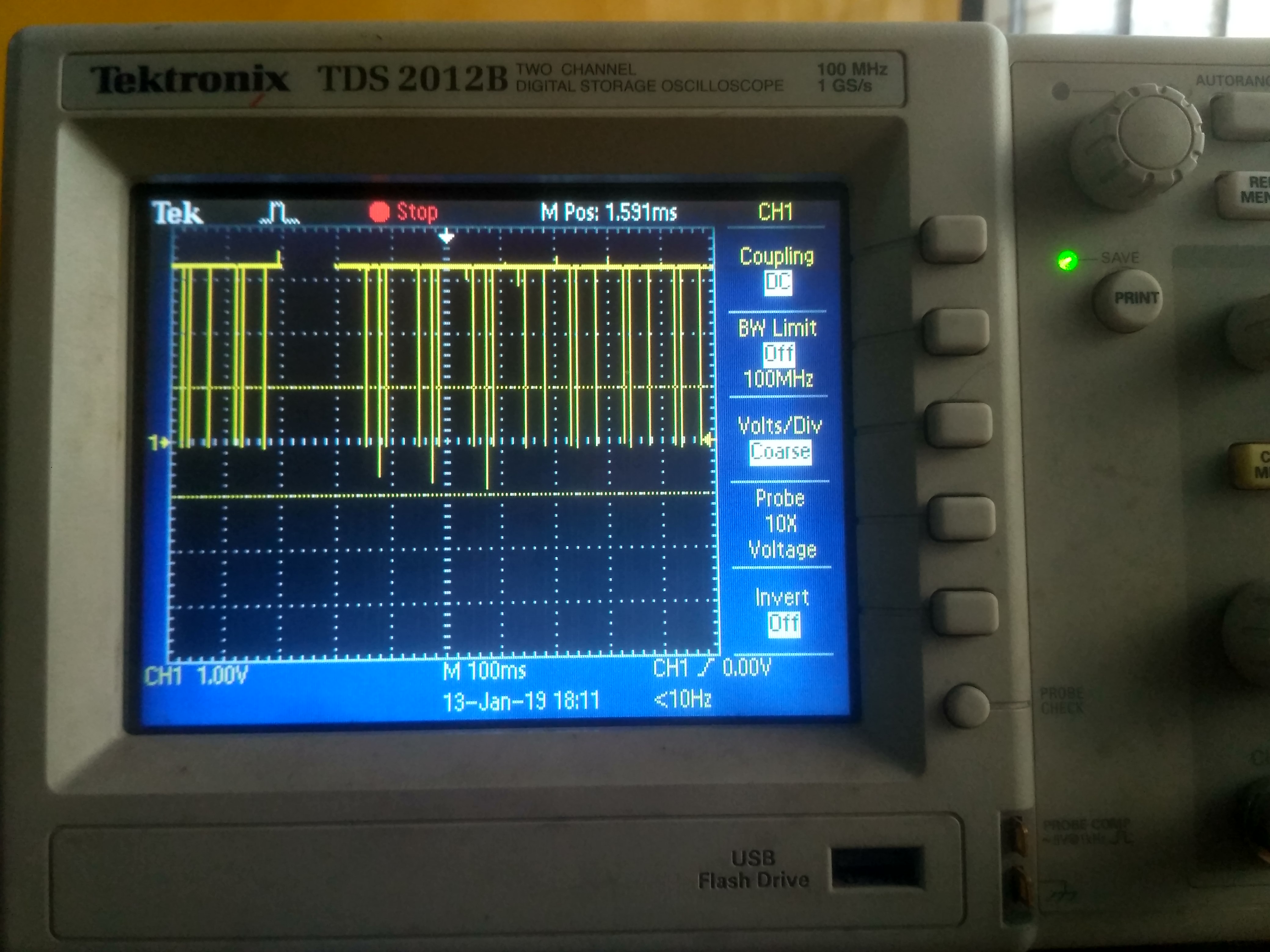
This is a example program in the C2000 examples but I have modified the pin numbers. I am only getting 3.3V constantly but not for some specified period is there any mistake in changing the pins or how the output should be if it is correct please help me.

#include "F28x_Project.h"

//
// Defines
//
#define DELAY (CPU_RATE/1000*6*510) //Qual period at 6 samples
//void delay ();
//
// Globals
//
volatile Uint32 Xint1Count;
volatile Uint32 Xint2Count;
Uint32 LoopCount;

//
// Function Prototypes
//
interrupt void xint1_isr(void);
interrupt void xint2_isr(void);

//
// Main
//
void main(void)
{
Uint32 TempX1Count;
Uint32 TempX2Count;

//
// Step 1. Initialize System Control:
// PLL, WatchDog, enable Peripheral Clocks
// This example function is found in the F2837xD_SysCtrl.c file.
//
InitSysCtrl();

//
// Step 2. Initialize GPIO:
// This example function is found in the F2837xD_Gpio.c file and
// illustrates how to set the GPIO to its default state.
//
// InitGpio(); // Skipped for this example

//
// Step 3. Clear all interrupts and initialize PIE vector table:
// Disable CPU interrupts
//
DINT;

//
// Initialize PIE control registers to their default state.
// The default state is all PIE interrupts disabled and flags
// are cleared.
// This function is found in the F2837xD_PieCtrl.c file.
//
InitPieCtrl();

//
// Disable CPU interrupts and clear all CPU interrupt flags:
//
IER = 0x0000;
IFR = 0x0000;

//
// Initialize the PIE vector table with pointers to the shell Interrupt
// Service Routines (ISR).
// This will populate the entire table, even if the interrupt
// is not used in this example. This is useful for debug purposes.
// The shell ISR routines are found in F2837xD_DefaultIsr.c.
// This function is found in F2837xD_PieVect.c.
//
InitPieVectTable();

//
// Interrupts that are used in this example are re-mapped to
// ISR functions found within this file.
//
EALLOW; // This is needed to write to EALLOW protected registers
PieVectTable.XINT1_INT = &xint1_isr;
PieVectTable.XINT2_INT = &xint2_isr;
EDIS; // This is needed to disable write to EALLOW protected registers

//
// Step 4. User specific code, enable interrupts:
//
// Clear the counters
//
Xint1Count = 0; // Count XINT1 interrupts
Xint2Count = 0; // Count XINT2 interrupts
LoopCount = 0; // Count times through idle loop

//
// Enable XINT1 and XINT2 in the PIE: Group 1 interrupt 4 & 5
// Enable INT1 which is connected to WAKEINT:
//
PieCtrlRegs.PIECTRL.bit.ENPIE = 1; // Enable the PIE block
PieCtrlRegs.PIEIER1.bit.INTx4 = 1; // Enable PIE Group 1 INT4
PieCtrlRegs.PIEIER1.bit.INTx5 = 1; // Enable PIE Group 1 INT5
IER |= M_INT1; // Enable CPU INT1
EINT; // Enable Global Interrupts

//
// GPIO30 & GPIO31 are outputs, start GPIO30 high and GPIO31 low
//
EALLOW;
GpioDataRegs.GPASET.bit.GPIO24 = 1; // Load the output latch
GpioCtrlRegs.GPAMUX2.bit.GPIO24 = 0; // GPIO
GpioCtrlRegs.GPADIR.bit.GPIO24 = 1; // output

GpioDataRegs.GPACLEAR.bit.GPIO29 = 1; // Load the output latch
GpioCtrlRegs.GPAMUX2.bit.GPIO29 = 0; // GPIO
GpioCtrlRegs.GPADIR.bit.GPIO29 = 1; // output
EDIS;

//
// GPIO0 and GPIO1 are inputs
//
EALLOW;
GpioCtrlRegs.GPAMUX1.bit.GPIO0 = 0; // GPIO
GpioCtrlRegs.GPADIR.bit.GPIO0 = 0; // input
GpioCtrlRegs.GPAQSEL1.bit.GPIO0 = 0; // XINT1 Synch to SYSCLKOUT only

GpioCtrlRegs.GPAMUX1.bit.GPIO1 = 0; // GPIO
GpioCtrlRegs.GPADIR.bit.GPIO1 = 0; // input
GpioCtrlRegs.GPAQSEL1.bit.GPIO1 = 2; // XINT2 Qual using 6 samples
GpioCtrlRegs.GPACTRL.bit.QUALPRD0 = 0xFF; // Each sampling window
// is 510*SYSCLKOUT
EDIS;

//
// GPIO0 is XINT1, GPIO1 is XINT2
//
GPIO_SetupXINT1Gpio(0);
GPIO_SetupXINT2Gpio(1);

//
// Configure XINT1
//
XintRegs.XINT1CR.bit.POLARITY = 0; // Falling edge interrupt
XintRegs.XINT2CR.bit.POLARITY = 1; // Rising edge interrupt

//
// Enable XINT1 and XINT2
//
XintRegs.XINT1CR.bit.ENABLE = 1; // Enable XINT1
XintRegs.XINT2CR.bit.ENABLE = 1; // Enable XINT2

//
// GPIO34 will go low inside each interrupt. Monitor this on a scope
//
EALLOW;
GpioCtrlRegs.GPBMUX2.bit.GPIO60 = 0; // GPIO
GpioCtrlRegs.GPBDIR.bit.GPIO60 = 1; // output
EDIS;

//
// Step 5. IDLE loop:
//
for(;;)
{
TempX1Count = Xint1Count;
TempX2Count = Xint2Count;

//
// Trigger both XINT1
//
GpioDataRegs.GPBSET.bit.GPIO60 = 1; // GPIO34 is high
GpioDataRegs.GPACLEAR.bit.GPIO30 = 1; // Lower GPIO30, trigger XINT1
while(Xint1Count == TempX1Count) {}

//
// Trigger both XINT2
//
GpioDataRegs.GPBSET.bit.GPIO60 = 1; // GPIO34 is high
DELAY_US(DELAY); // Wait for Qual period
GpioDataRegs.GPASET.bit.GPIO31 = 1; // Raise GPIO31, trigger XINT2
while(Xint2Count == TempX2Count) {}

//
// Check that the counts were incremented properly and get ready
// to start over.
//
if(Xint1Count == TempX1Count + 1 && Xint2Count == TempX2Count + 1)
{
LoopCount++;
GpioDataRegs.GPASET.bit.GPIO30 = 1; // raise GPIO30
GpioDataRegs.GPACLEAR.bit.GPIO31 = 1; // lower GPIO31
}
else
{
asm(" ESTOP0"); // stop here
}
}
}

//
// xint1_isr - External Interrupt 1 ISR
//
interrupt void xint1_isr(void)
{
GpioDataRegs.GPBCLEAR.all = 0x0000; // GPIO34 is low
Xint1Count++;

//
// Acknowledge this interrupt to get more from group 1
//
PieCtrlRegs.PIEACK.all = PIEACK_GROUP1;
}

//
// xint2_isr - External Interrupt 2 ISR
//
interrupt void xint2_isr(void)
{
GpioDataRegs.GPBCLEAR.all = 0x0000; // GPIO34 is low
Xint2Count++;

//
// Acknowledge this interrupt to get more from group 1
//
PieCtrlRegs.PIEACK.all = PIEACK_GROUP1;
}

  • Panda,

    Please explain in detail what you are trying to do. We can't go through the code to figure that out.

    Regards,
    Manoj
  • Manoj,

    I want to know what should be my output, as i am getting a constant 3.3V output, how can I get a pulsed output by adjusting the delay() function or by adjusting the sampling time.

    Thank you
    Bighnaraj Panda
  • Manoj,
    I have given different values in the delay(1000) and delay(250) and also the value given in the example program functions but the output is not changing. I have also adjusted the number of samples as synchronous with the sysclock

    GpioCtrlRegs.GPAQSEL1.bit.GPIO1 = 2; // XINT2 Qual using 6 samples

    but still there is no effect on the output. Please help me to find the fault.

    Thank you
    Bighnaraj Panda
  • Panda,

    I believe this is what you are trying to do:-

    1) GPIO0 is configured to trigger XINT1 and GPIO1 is configured to trigger XINT2
    2) GPIO24 and GPIO29 is configured as GPIO output pin.
    3) GPIO24 is connected to GPIO0 pin
    4) GPIO29 is connected to GPIO1 pin
    5) Use GPIO34 to monitor in scope.

    Corrected code:

    #include "F28x_Project.h"

    //
    // Defines
    //
    #define DELAY (CPU_RATE/1000*6*510) //Qual period at 6 samples
    //void delay ();
    //
    // Globals
    //
    volatile Uint32 Xint1Count;
    volatile Uint32 Xint2Count;
    Uint32 LoopCount;

    //
    // Function Prototypes
    //
    interrupt void xint1_isr(void);
    interrupt void xint2_isr(void);

    //
    // Main
    //
    void main(void)
    {
    Uint32 TempX1Count;
    Uint32 TempX2Count;

    //
    // Step 1. Initialize System Control:
    // PLL, WatchDog, enable Peripheral Clocks
    // This example function is found in the F2837xD_SysCtrl.c file.
    //
    InitSysCtrl();

    //
    // Step 2. Initialize GPIO:
    // This example function is found in the F2837xD_Gpio.c file and
    // illustrates how to set the GPIO to its default state.
    //
    // InitGpio(); // Skipped for this example

    //
    // Step 3. Clear all interrupts and initialize PIE vector table:
    // Disable CPU interrupts
    //
    DINT;

    //
    // Initialize PIE control registers to their default state.
    // The default state is all PIE interrupts disabled and flags
    // are cleared.
    // This function is found in the F2837xD_PieCtrl.c file.
    //
    InitPieCtrl();

    //
    // Disable CPU interrupts and clear all CPU interrupt flags:
    //
    IER = 0x0000;
    IFR = 0x0000;

    //
    // Initialize the PIE vector table with pointers to the shell Interrupt
    // Service Routines (ISR).
    // This will populate the entire table, even if the interrupt
    // is not used in this example. This is useful for debug purposes.
    // The shell ISR routines are found in F2837xD_DefaultIsr.c.
    // This function is found in F2837xD_PieVect.c.
    //
    InitPieVectTable();

    //
    // Interrupts that are used in this example are re-mapped to
    // ISR functions found within this file.
    //
    EALLOW; // This is needed to write to EALLOW protected registers
    PieVectTable.XINT1_INT = &xint1_isr;
    PieVectTable.XINT2_INT = &xint2_isr;
    EDIS; // This is needed to disable write to EALLOW protected registers

    //
    // Step 4. User specific code, enable interrupts:
    //
    // Clear the counters
    //
    Xint1Count = 0; // Count XINT1 interrupts
    Xint2Count = 0; // Count XINT2 interrupts
    LoopCount = 0; // Count times through idle loop

    //
    // Enable XINT1 and XINT2 in the PIE: Group 1 interrupt 4 & 5
    // Enable INT1 which is connected to WAKEINT:
    //
    PieCtrlRegs.PIECTRL.bit.ENPIE = 1; // Enable the PIE block
    PieCtrlRegs.PIEIER1.bit.INTx4 = 1; // Enable PIE Group 1 INT4
    PieCtrlRegs.PIEIER1.bit.INTx5 = 1; // Enable PIE Group 1 INT5
    IER |= M_INT1; // Enable CPU INT1
    EINT; // Enable Global Interrupts

    //
    // GPIO24 & GPIO29 are outputs, start GPIO24 high and GPIO29 low
    //
    EALLOW;
    GpioDataRegs.GPASET.bit.GPIO24 = 1; // Load the output latch
    GpioCtrlRegs.GPAMUX2.bit.GPIO24 = 0; // GPIO
    GpioCtrlRegs.GPADIR.bit.GPIO24 = 1; // output

    GpioDataRegs.GPACLEAR.bit.GPIO29 = 1; // Load the output latch
    GpioCtrlRegs.GPAMUX2.bit.GPIO29 = 0; // GPIO
    GpioCtrlRegs.GPADIR.bit.GPIO29 = 1; // output
    EDIS;

    //
    // GPIO0 and GPIO1 are inputs
    //
    EALLOW;
    GpioCtrlRegs.GPAMUX1.bit.GPIO0 = 0; // GPIO
    GpioCtrlRegs.GPADIR.bit.GPIO0 = 0; // input
    GpioCtrlRegs.GPAQSEL1.bit.GPIO0 = 0; // XINT1 Synch to SYSCLKOUT only

    GpioCtrlRegs.GPAMUX1.bit.GPIO1 = 0; // GPIO
    GpioCtrlRegs.GPADIR.bit.GPIO1 = 0; // input
    GpioCtrlRegs.GPAQSEL1.bit.GPIO1 = 2; // XINT2 Qual using 6 samples
    GpioCtrlRegs.GPACTRL.bit.QUALPRD0 = 0xFF; // Each sampling window
    // is 510*SYSCLKOUT
    EDIS;

    //
    // GPIO0 is XINT1, GPIO1 is XINT2
    //
    GPIO_SetupXINT1Gpio(0);
    GPIO_SetupXINT2Gpio(1);

    //
    // Configure XINT1
    //
    XintRegs.XINT1CR.bit.POLARITY = 0; // Falling edge interrupt
    XintRegs.XINT2CR.bit.POLARITY = 1; // Rising edge interrupt

    //
    // Enable XINT1 and XINT2
    //
    XintRegs.XINT1CR.bit.ENABLE = 1; // Enable XINT1
    XintRegs.XINT2CR.bit.ENABLE = 1; // Enable XINT2

    //
    // GPIO60 will go low inside each interrupt. Monitor this on a scope
    //
    EALLOW;
    GpioCtrlRegs.GPBMUX1.bit.GPIO34 = 0; // GPIO
    GpioCtrlRegs.GPBDIR.bit.GPIO34 = 1; // output
    EDIS;

    //
    // Step 5. IDLE loop:
    //
    for(;;)
    {
    TempX1Count = Xint1Count;
    TempX2Count = Xint2Count;

    //
    // Trigger both XINT1
    //
    GpioDataRegs.GPBSET.bit.GPIO34 = 1; // GPIO34 is high
    GpioDataRegs.GPACLEAR.bit.GPIO24 = 1; // Lower GPIO24, trigger XINT1
    while(Xint1Count == TempX1Count) {}

    //
    // Trigger both XINT2
    //
    GpioDataRegs.GPBSET.bit.GPIO34 = 1; // GPIO34 is high
    DELAY_US(DELAY); // Wait for Qual period
    GpioDataRegs.GPASET.bit.GPIO29 = 1; // Raise GPIO29, trigger XINT2
    while(Xint2Count == TempX2Count) {}

    //
    // Check that the counts were incremented properly and get ready
    // to start over.
    //
    if(Xint1Count == TempX1Count + 1 && Xint2Count == TempX2Count + 1)
    {
    LoopCount++;
    GpioDataRegs.GPASET.bit.GPIO24 = 1; // raise GPIO24
    GpioDataRegs.GPACLEAR.bit.GPIO29 = 1; // lower GPIO29
    }
    else
    {
    asm(" ESTOP0"); // stop here
    }
    }
    }

    //
    // xint1_isr - External Interrupt 1 ISR
    //
    interrupt void xint1_isr(void)
    {
    GpioDataRegs.GPBCLEAR.bit.GPIO34 = 1; // GPIO60 is low
    Xint1Count++;

    //
    // Acknowledge this interrupt to get more from group 1
    //
    PieCtrlRegs.PIEACK.all = PIEACK_GROUP1;
    }

    //
    // xint2_isr - External Interrupt 2 ISR
    //
    interrupt void xint2_isr(void)
    {
    GpioDataRegs.GPBCLEAR.bit.GPIO34 = 1; // GPIO60 is low
    Xint2Count++;

    //
    // Acknowledge this interrupt to get more from group 1
    //
    PieCtrlRegs.PIEACK.all = PIEACK_GROUP1;
    }

    Regards,
    Manoj
  • Manoj,
    I have set the SYSCLKOUT frequency at 200MHz and a delay of (1000*6*510). The output is the image in which I am not able to understand the output. Can you please make me understand how this output is related to the programming input.

    Thank you
    Bighnaraj Panda
  • Panda,

    According to the example, GPIO34 will not toggle unless XINT1 and XINT2 interrupt are triggered. GPIO0 triggers XINT1 and GPIO1 triggers XINT2 interrupt.

    Regards,
    Manoj
  • Manoj,
    You mean to say that in my program the interrupt is not getting triggered? But I have connected GPIO0 to GPIO24 and GPIO1 to GPIO29 externally and connected the probe to GPIO34. Then XINT1 and XINT2 interrupt are not triggered.

    Thank you
    Bighnaraj Panda
  • Panda,

    As I mentioned before, there were some configuration issues in your code and external interrupts weren't getting generated.

    Regards,
    Manoj
  • Still the program is not running correctly as mentioned above due to some configuration issues how to sort out those issues please help me.

    Thank you
    Bighnaraj Panda
  • Panda,

    Please explain the problem.

    Regards,
    Manoj
  • Panda,

    Are you saying that modified program I gave is also not working? Your oscilloscope snapshot seems to suggest that the code is working.

    Before I sent you the code, I made sure that the code is working.

    Regards,
    Manoj