This thread has been locked.

If you have a related question, please click the "Ask a related question" button in the top right corner. The newly created question will be automatically linked to this question.

TMS320F28069M: SPI is inserting an extra bit in front of read transfer

Part Number: TMS320F28069M
Other Parts Discussed in Thread: TMS320F28027, LAUNCHXL-F28027F, LAUNCHXL-F28069M

I am upgrading from the TMS320F28027 to the '069 and SPI code that worked there is not working on the new chip. 

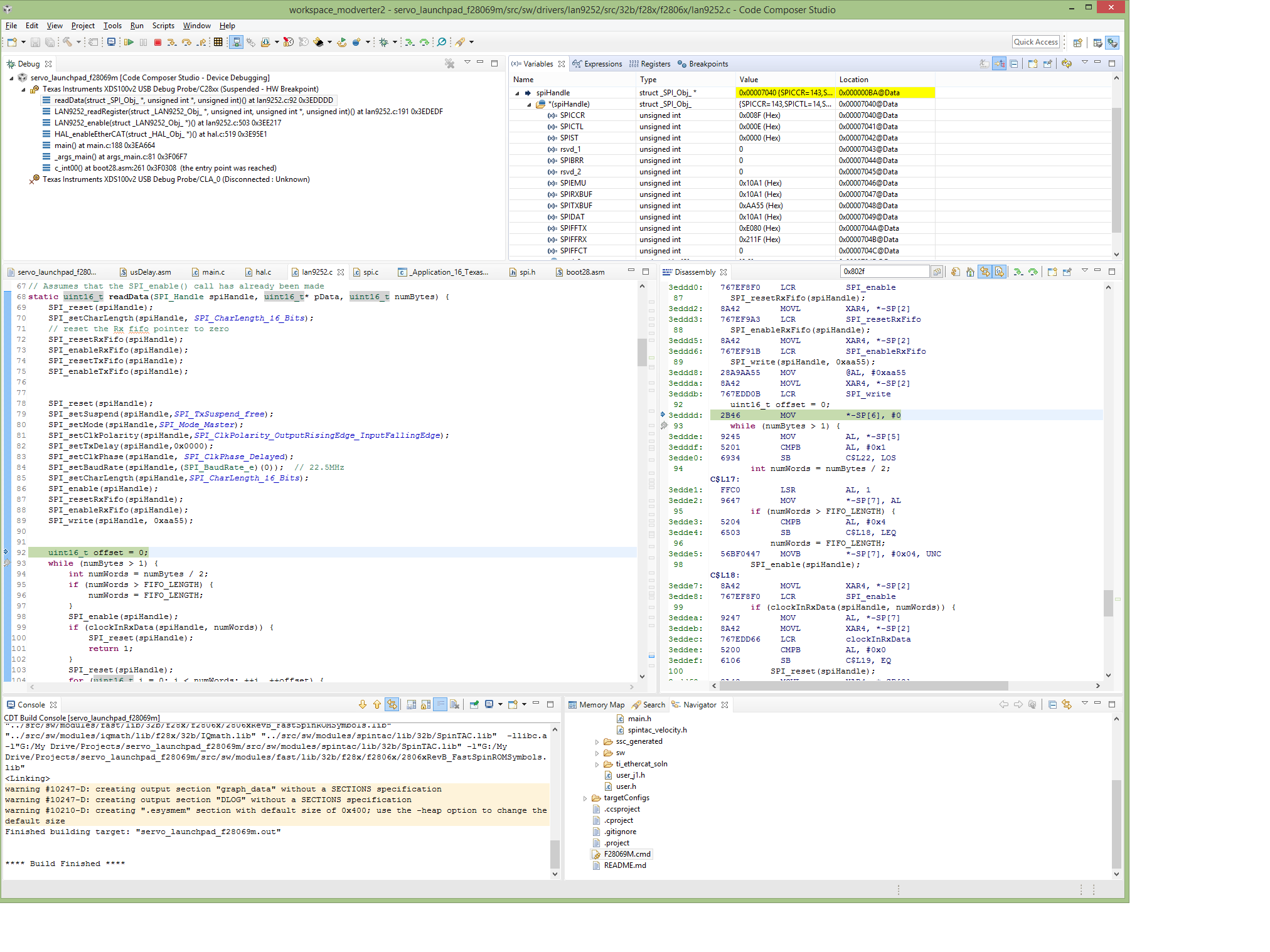
The error is that there is an extra bit inserted at the front of the data transfer that is not seen in the actual data transfer. The data received is 0x10a1 rather than the transmitted data 0x2143. Note that 0x10a1 == (0x2143 >> 1).

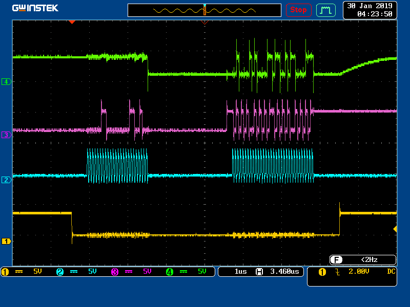
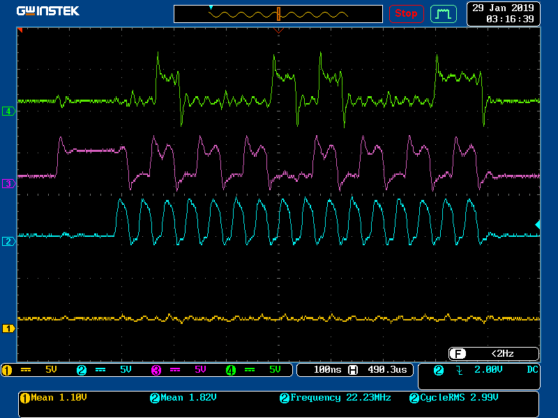
I am attaching an oscilloscope capture of the trace as seen on the SPI lines. The signals from top to bottom are SIMO (green) clocking in the bit pattern 0010-0001-0100-0011 (0x2143), SOMI (purple) clocking out the bit pattern 1010-1010-0101-0101 (0xaa55), SCLK (blue), and SCS (yellow) which is low throughout the transfer.

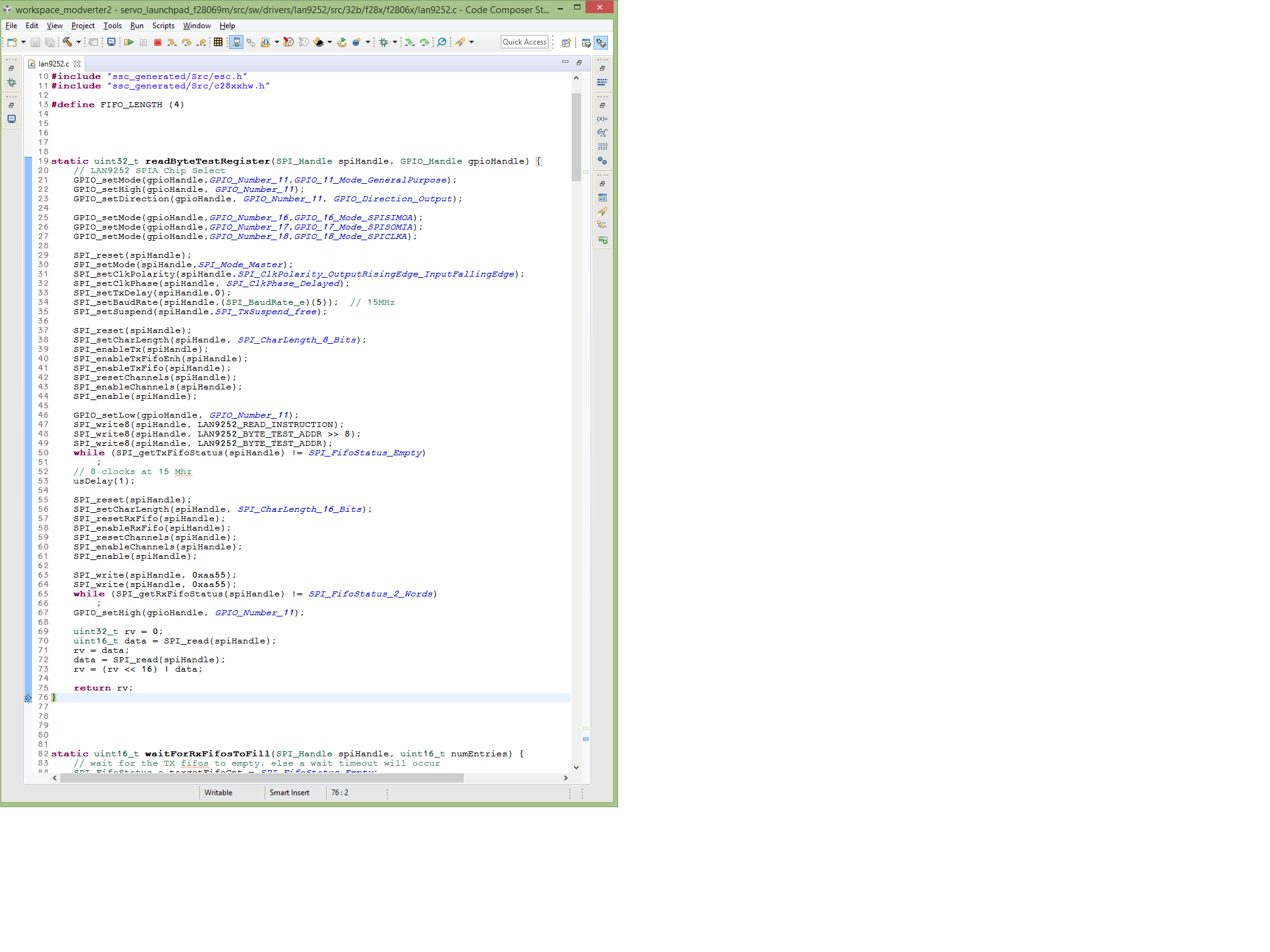
The SPI configuration is shown in the next screen capture which shows the setup and transfer code as well as the SPI registers immediately following the transfer. I am configuring the clock to capture input data on the rising edge of the clock Polarity=0, Phase=1.
  • Craig,

    Please confirm that the only thing changed is the MCU. From F28027 to F28069?
    Usually when this occurs, it is because the SPI modules have lost word synchronization with each other. Your chip select signal is low for the full screen capture, at least, do you toggle the chip select line between transmissions?
    Your C2000 is a SPI master, what is the SPI slave? is it another MCU? An External DAC, ADC, Flash?
    Which GPIOs are being used? Certain GPIOs may be in a different state at power up between F28027 and F28069. Meaning, if your SPI slave is waiting and chip select is enabled by the time the Master device reconfigures the pin which will be SPICLK, you may have an extra toggle, which the slave will interpret as valid and clock a bit.

    Regards,
    Mark
  • Mark,

    Thanks for the prompt reply. The SPI slave we are using is a dedicated SPI slave chip from another vendor. The F28027 code was developed first on a launchxl-f28027f connected to the their development board by jumpering the SPI signals and Ground wires. Later we spun our own board with a 28027f and verified that the code continued to function properly. Now that we are changing to the 28069M I am using the launchxl-f28069m board connected back to the original slave development board and the same jumpers (with more grounding). I did change the CS* line from GPIO_Number_19 to GPIO_Number_11.

    I have rewritten the code into a single function below so that you can see the entire GPIO/SPI configuration and the transfer. The traces below are generated by this code. As you can see, the CS* line never rises and there are no extra clocks. The received value from the code is 0x10A1B2C3 which is the transferred value of 0x21436587 >> 1.

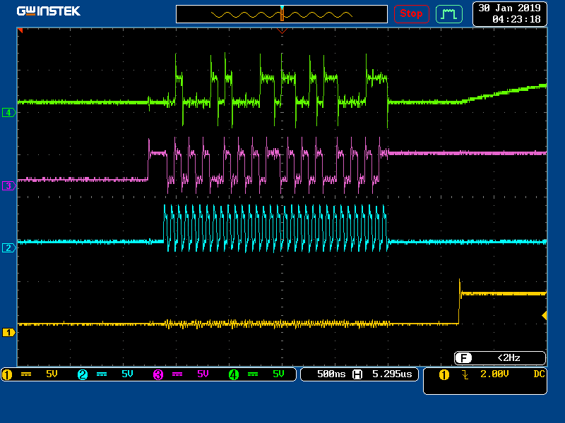
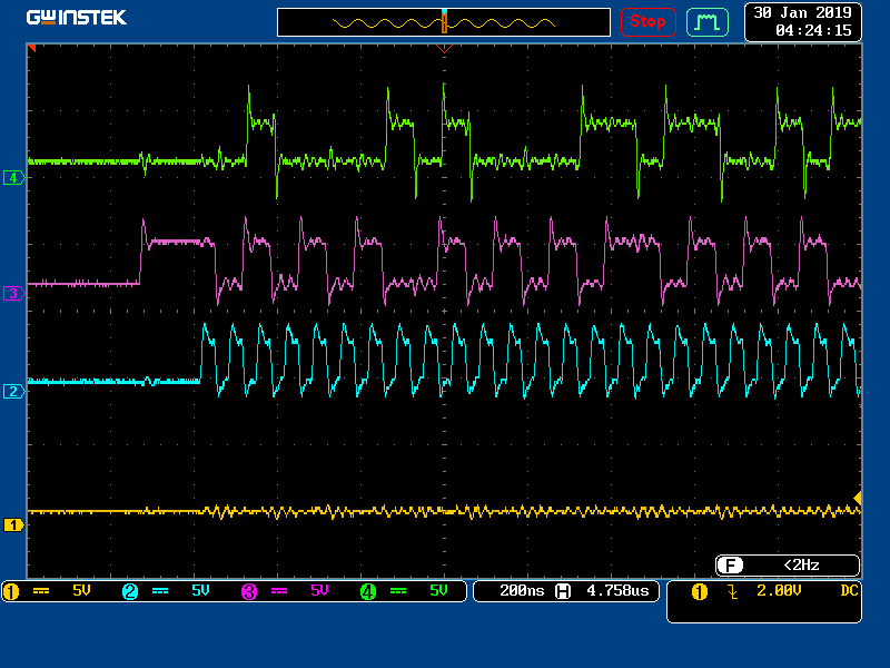
    The transfer consists of the Master sending three bytes: 0x03 for a Read; 0x00 as high byte register address; 0x64 as low byte; In response the slave sends the response 0x21436587 (00100001 01000011 01100101 10000111). All of this can be seen in the traces below.

    Complete transfer

    Read Command and Address (0x03, 0x00, 0x64) zoomed in

    Response data as 8-bit transfers (0x21, 0x43, 0x65, 0x87) zoomed in

    Initial part of Response data zoomed in

  • Hi Craig,

    Sorry for the delay. Looking through the code, and captures, everything appears to be in order.
    Though you are reconfiguring the SPI word length mid-transaction, you are doing it properly by putting the module in reset, changing config, then re-enabling. Personally, i would just keep it all in an 8-bit word format, but again, the way you are doing this is correct.

    Your SPI configuration is "Rising Edge with Delay" which by the TRM definition is " The SPI transmits data one half-cycle ahead of the rising edge of the SPICLK signal and receives data on the rising edge of the SPICLK signal."Tracing this out on the scope captures shows that you see both the SIMO data (purple) and SOMI data (green) changing on the falling edge (half cycle ahead). The SPI will sample the SOMI line on the rising edge. SPISTE is toggling appropriately, and there are no extra clocks. This all appears to line up correctly.

    Can you try the following tests?
    1. Use the same SPI configuration and transfer code on the F28027F- show the screen captures.
    2. Add 2 NOPs between re-enabling the SPI and sending the 16-bit dummy words.
    3. Use 8-bit word length only, no reconfiguring the SPI mid-transaction.

    Thanks,
    Mark
  • Hi Mark,

    I did as you requested. The NOPs and the 8-bit transfers had no effect. Then I tried running the code on the 28027F and got the same failure, an extra bit shifted in ahead of the true bits.

    I was then able to track it down to the SPIBRR, baud rate register. On the 28027F the transfer fails when the SPIBRR is assigned a value of 5 or less. On the 28069M the failures occur at values of 9 and below. (Thankfully I wasn't using values of 6, 7, 8, or 9 on the 28069M or the code that failed on the 28069M would have run on the 28027F successfully!)

    Using the configuration I have shouldn't both chips be able to run correctly with SPIBRR values all the way down to 0? Did I miss something in the Technical Reference or in an Application Note?

    Thanks for helping me track this down.

    -Craig

  • Craig,

    The SPI operates at LSPCLK/(SPIBRR+1). If SPIBRR <= 3, it is LSPCLK/4. This is documented in both the datasheet and the TRM.
    Depending on your PLL frequency and LSPCLKDIV, you were likely operating at different SPI frequencies. You could potentially be violating the Setup and hold timings of the SPISOMI signal.

    According to the F28069M datasheet in the "SPI Master Mode Electrical Data/Timing" section , the theoretical maximum SPI master receive frequency is 12.5Mhz. The reason I say "theoretical" is that is what the device is capable of achieving if all timings are met. You would need to ensure that your signals are clean and any other board/system level delays match.

    -Mark
  • Mark,

    I never looked past the max frequency of LSPCLK/4 in the Tech Ref, so I didn't confirm the setup time in the Datasheet. The Datasheet says that with my clock configuration the data has to be valid within 10nsec of the falling clock edge. The SPI slave I use has a max delay time of 11nsec. Apparently that was enough to mess me up at high frequencies. Changing the clocking scheme of the SPI now allows me to go up to the max frequency (i.e. up to 12.5MHz).

    Thanks for all your help,
    Craig
  • Craig,
    I am glad to hear that this was it!

    If you have more questions in the future, please don't hesitate to post again.

    Thanks,
    Mark