Part Number: TMS320F28069
Tool/software: Code Composer Studio
Hi,
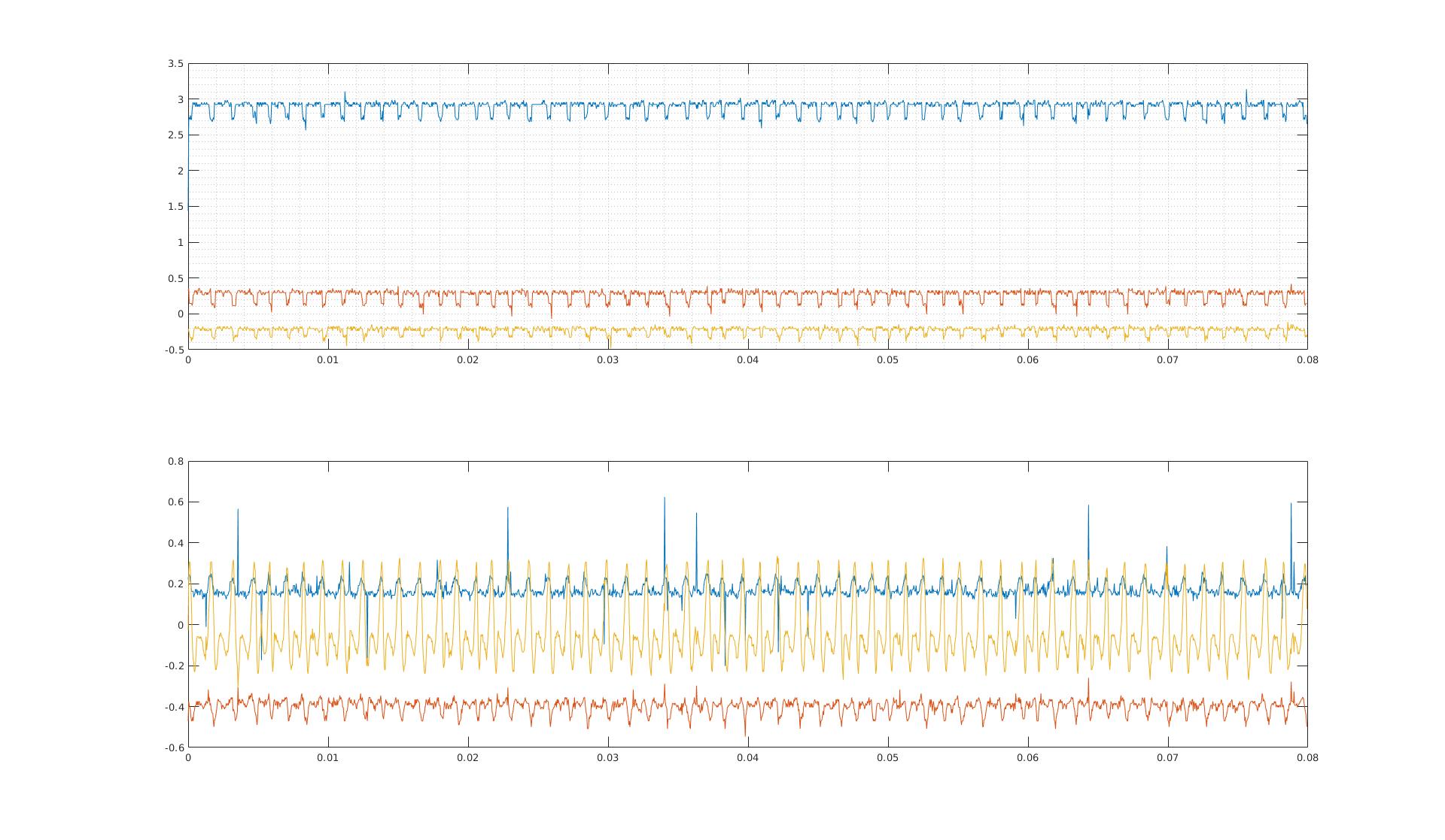
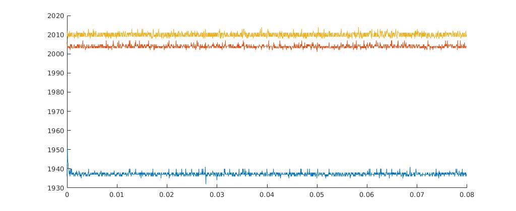
My team and i have developed a 3-phase motor controller, using the F28069 DSP. We have some issues with approximately 1kHz periodic noise signal, which appears on the measured phase currents even if all mosfets are fully off (0% duty cycle) or fully on (100% duty cycle). To investigate this event further, we have tried measuring the phase currents with some external in-line hall effect sensors instead of the on-board low-side shunt-resistors. The 1kHz appears here as well - however not when the external sensors are connected to the ADC B group instead of the A group on the DSP.
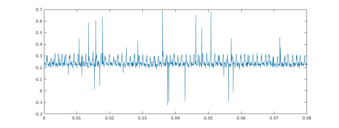
When i sample signals using the external sensors, which are connected to ADC A4, A5 and A6 channels, an approximately 1kHz periodic noise appear.
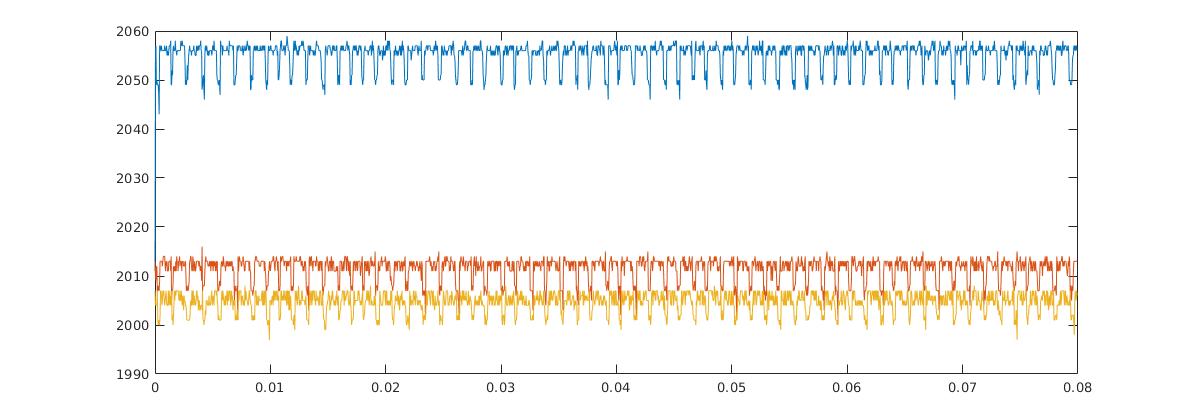
When i connect the exact same sensors to the ADC B3, B4, B5 the problem seems to disappear.
Any ideas what could be the problem?
This is my ADC configuration (initADC()) and how i read from the sensors (readPhaseCurrentsExtern()):
#define ACQPS_VALUE 6

void InitADC() {

    InitAdc();
    InitAdcAio();
    //AdcOffsetSelfCal();
    // Configure ADC
    EALLOW;
    AdcRegs.ADCCTL2.bit.ADCNONOVERLAP = 1;   //Enable non-overlap mode
    AdcRegs.ADCSOC0CTL.bit.CHSEL  = 0;       //Set SOC0 channel select to ADCINA0
    AdcRegs.ADCSOC0CTL.bit.TRIGSEL = 5;
    AdcRegs.ADCSOC0CTL.bit.ACQPS  = ACQPS_VALUE;      //Set SOC0 acquisition period to 26 ADCCLK

    AdcRegs.ADCSOC1CTL.bit.CHSEL  = 1;       //Set SOC0 channel select to ADCINA1
    AdcRegs.ADCSOC1CTL.bit.TRIGSEL = 5;
    AdcRegs.ADCSOC1CTL.bit.ACQPS  = ACQPS_VALUE;      //Set SOC0 acquisition period to 26 ADCCLK

    AdcRegs.ADCSOC2CTL.bit.CHSEL  = 2;       //Set SOC0 channel select to ADCINA2
    AdcRegs.ADCSOC2CTL.bit.TRIGSEL = 5;
    AdcRegs.ADCSOC2CTL.bit.ACQPS  = ACQPS_VALUE;      //Set SOC0 acquisition period to 26 ADCCLK

    AdcRegs.ADCSOC9CTL.bit.CHSEL  = 4;       //Set SOC0 channel select to ADCINA3
    AdcRegs.ADCSOC9CTL.bit.TRIGSEL = 5;
    AdcRegs.ADCSOC9CTL.bit.ACQPS  = ACQPS_VALUE;      //Set SOC0 acquisition period to 26 ADCCLK

    AdcRegs.ADCSOC10CTL.bit.CHSEL  = 5;       //Set SOC0 channel select to ADCINA3
    AdcRegs.ADCSOC10CTL.bit.TRIGSEL = 5;
    AdcRegs.ADCSOC10CTL.bit.ACQPS  = ACQPS_VALUE;      //Set SOC0 acquisition period to 26 ADCCLK

    AdcRegs.ADCSOC11CTL.bit.CHSEL  = 6;       //Set SOC0 channel select to ADCINA3
    AdcRegs.ADCSOC11CTL.bit.TRIGSEL = 5;
    AdcRegs.ADCSOC11CTL.bit.ACQPS  = ACQPS_VALUE;      //Set SOC0 acquisition period to 26 ADCCLK

    EDIS;

    /* Set up Event Trigger with CNT_zero enable for Time-base of EPWM1 */                      \
    EPwm1Regs.ETSEL.bit.SOCAEN = 1;     /* Enable SOCA */                                       \
    EPwm1Regs.ETSEL.bit.SOCASEL = 1;    /* Enable CNT_zero event for SOCA */                    \
    EPwm1Regs.ETPS.bit.SOCAPRD = 1;     /* Generate SOCA on the 1st event */                    \
    EPwm1Regs.ETCLR.bit.SOCA = 1;       /* Clear SOCA flag */
}

Phase readPhaseCurrentsExtern() {
    Phase current;

    //Fetch ADC values from data registers
    current.a = AdcResult.ADCRESULT9;
    current.b = AdcResult.ADCRESULT10;
    current.c = AdcResult.ADCRESULT11;

    return current;
}
where the InitAdc() and InitAdcAio() is:
void InitAdc(void)
{
extern void DSP28x_usDelay(Uint32 Count);
// *IMPORTANT*
// The Device_cal function, which copies the ADC calibration values from TI reserved
// OTP into the ADCREFSEL and ADCOFFTRIM registers, occurs automatically in the
// Boot ROM. If the boot ROM code is bypassed during the debug process, the
// following function MUST be called for the ADC to function according
// to specification. The clocks to the ADC MUST be enabled before calling this
// function.
// See the device data manual and/or the ADC Reference
// Manual for more information.
EALLOW;
SysCtrlRegs.PCLKCR0.bit.ADCENCLK = 1;
(*Device_cal)();
EDIS;
DELAY_US(ADC_usDELAY);
AdcRegs.ADCCTL1.all=ADC_RESET_FLAG;
asm(" NOP ");
asm(" NOP ");
EALLOW;
AdcRegs.ADCCTL1.bit.ADCBGPWD = 1; /* Power up band gap */
DELAY_US(ADC_usDELAY); /* Delay before powering up rest of ADC */
AdcRegs.ADCCTL1.bit.ADCREFSEL = 0;
AdcRegs.ADCCTL1.bit.ADCREFPWD = 1; /* Power up reference */
AdcRegs.ADCCTL1.bit.ADCPWDN = 1; /* Power up rest of ADC */
AdcRegs.ADCCTL1.bit.ADCENABLE = 1; /* Enable ADC */
asm(" RPT#100 || NOP");
AdcRegs.ADCCTL1.bit.INTPULSEPOS=1;
AdcRegs.ADCCTL1.bit.TEMPCONV=0;
DELAY_US(ADC_usDELAY);
}
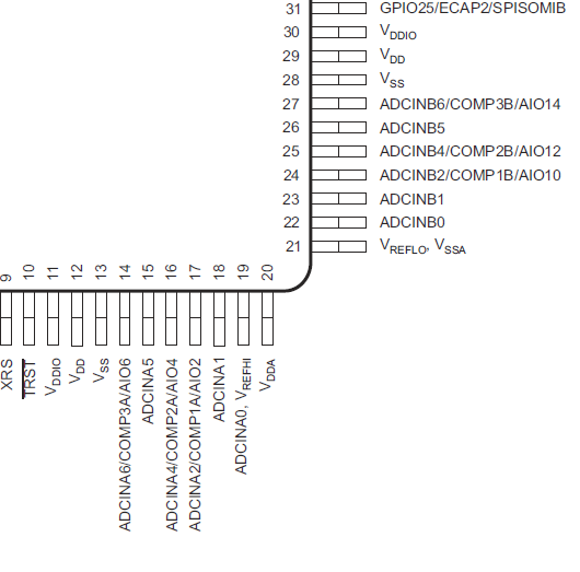
void InitAdcAio()
{
EALLOW;
GpioCtrlRegs.AIODIR.all = 0x0000;
/* Configure ADC pins using AIO regs*/
// This specifies which of the possible AIO pins will be Analog input pins.
// NOTE: AIO1,3,5,7-9,11,13,15 are analog inputs in all AIOMUX1 configurations.
// Comment out other unwanted lines.
GpioCtrlRegs.AIOMUX1.bit.AIO2 = 2; // Configure AIO2 for A2 (analog input) operation
GpioCtrlRegs.AIOMUX1.bit.AIO4 = 2; // Configure AIO4 for A4 (analog input) operation
GpioCtrlRegs.AIOMUX1.bit.AIO6 = 2; // Configure AIO6 for A6 (analog input) operation
GpioCtrlRegs.AIOMUX1.bit.AIO10 = 2; // Configure AIO10 for B2 (analog input) operation
GpioCtrlRegs.AIOMUX1.bit.AIO12 = 2; // Configure AIO12 for B4 (analog input) operation
GpioCtrlRegs.AIOMUX1.bit.AIO14 = 2; // Configure AIO14 for B6 (analog input) operation
EDIS;
}