This thread has been locked.

If you have a related question, please click the "Ask a related question" button in the top right corner. The newly created question will be automatically linked to this question.

TMS320F28023: The product doesn`t pass parametrical control.

Part Number: TMS320F28023


Greetings!

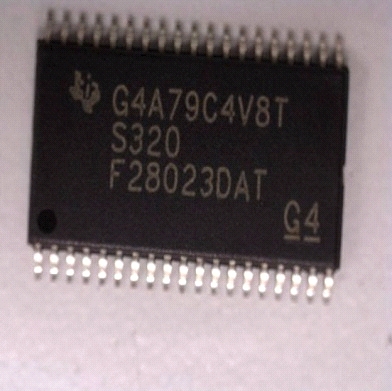
Part. number TMS320F28023DAT.

Out of 38 pieces from the order, there are no pieces that passed parametrical control.

The product doesn`t pass parametrical control.
The core voltage controller does not work
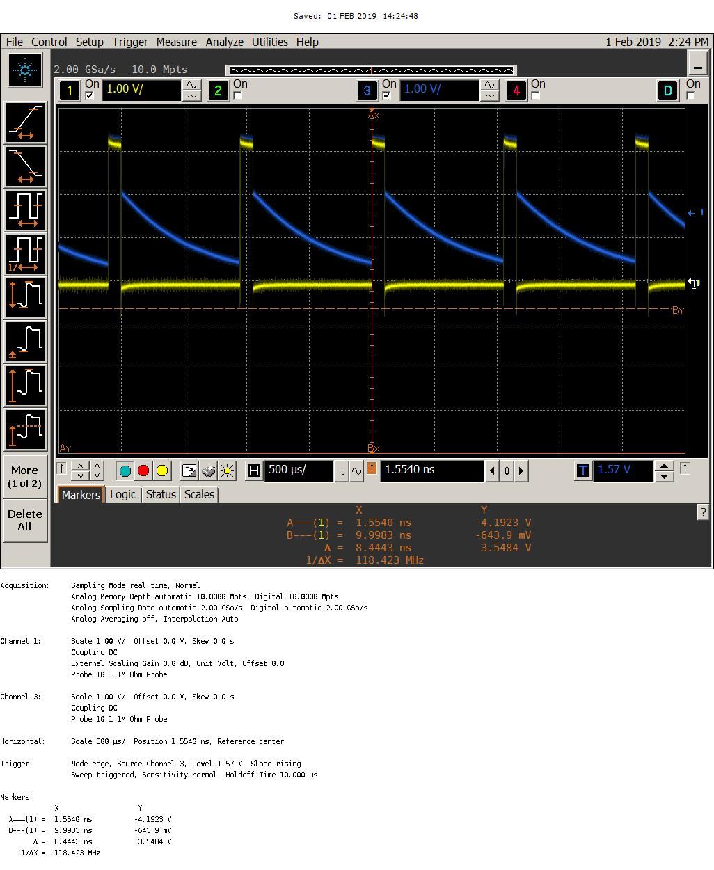
If core has external supply voltage, microchip is constantly reset on watchdog timer with a period of 1 µs
The scheme of inclusion in the mode of external core supply is on pic.1
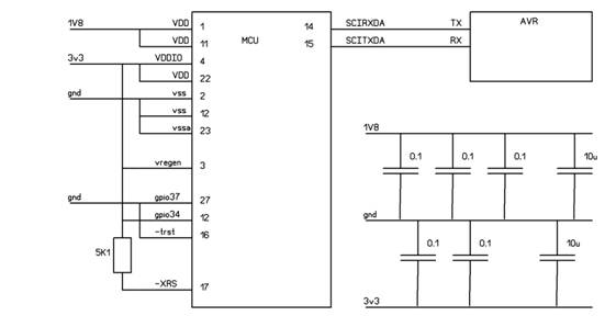
pic.1

Is there any solution of the problem or it`s production defect ?

  • Please answer each one of the below questions clearly, in order to help you better:

    • Could you please clarify what you mean by “parametrical control”? What is tested?
    • Is there any code residing in the MCU?
    • Is there any other hardware connected to the MCU?
    • What do you mean by “The core voltage controller does not work”?
    • A reset period if 1 uS cannot be from the internal watchdog. Are you referring to an external watchdog IC?
    • I notice that –TRST is directly connected to GND. Although the chip can execute code in this configuration, you will not be able to connect any debug probe (like XDS100) to the JTAG port. Such debug probes would attempt to drive the –TRST pin high and it will likely result in damage of the probe.

  • 1. Сompliance of electrical characteristics mentioned in datasheet was tested.

    2. There was no code in the MCU.

    3. The device imitating initial loading was connected on UART.

    4. It means that on the inputs, which should have 1.8 V supply voltage, there is no corresponding constant voltage at an operation mode from the built-in regulator. (May be there was missanderstanding because of incorrect translation: The core voltage controller - Regulator of the voltage of the core)

    5.No, there was no external watchdog.

    6. Debug probe was not used during testing.
  • 1. Сompliance of electrical characteristics mentioned in datasheet was tested.

    I regret I still don’t understand what you mean by this. Unless you explain what exactly you are testing and how, I will not be able to help. All devices that are shipped from the factory have passed our production tests. It is inconceivable that you received 38 devices and all of them are bad.


    2. There was no code in the MCU.

    OK. Flash is erased.


    3. The device imitating initial loading was connected on UART.

    What is the objective of connecting the SCI pins to an external UART?


    4. It means that on the inputs, which should have 1.8 V supply voltage, there is no corresponding constant voltage at an operation mode from the built-in regulator. (May be there was missanderstanding because of incorrect translation: The core voltage controller - Regulator of the voltage of the core)

    Are you saying when VREGENZ was connected to GND, the internal VREG did not output 1.8v on the VDD pins? Can you send me the schematics of your board privately?


    5.No, there was no external watchdog.

    As explained before, a reset period if 1 uS cannot be from the internal watchdog. How did you determine it is from the internal WD? Where did you measure the waveform? Can you attach oscilloscope plots?


    6. Debug probe was not used during testing.

    Did you try connecting the device to CCS via a debug probe like XDS100?

  •  1. Consumption current, logic-1 level and functional control was cheked.

    3. The main objective is to get a response on boot sequence.

    4. Voltage on Vdd fluctuates from 1.8V to 3.3.V. There is no constant  voltage 1.8V.

    Microchip was installed only into DIP-panel, so the scheme is in the very first message.

    5. The assumption that microchip is reset on internal watchdog timer  made because of we have no other assumptions.

    We measured the waveform after connecting supply voltage.

    6. No,we didn`t.

  • Which pin was the waveform measured? There are 2 waveforms (blue and yellow). Neither of them look like they were produced by the internal watchdog. The XRS pin will be normally high and will pulse low (for a duration of 512 OSCCLK cycles) if activated by the WD.

    Your boot-mode pins are configured correctly for SCI, but what data are you trying to transfer from the AVR chip? Does that code contain the needed headers? See SPRUI09 for information.

    Is the behavior identical whether or not the internal VREG is used?

    I suggest you mount the chip on the PCB and attempt to connect via JTAG using CCS.

    With the limited information you have provided, I am unable to suggest anything beyond this.
  •  1. The yellow waveform measured from xrs pin, blue – from GPIO29/SCI TXDA/SCLA/TZ3 15

    The described situation with xrs pin does not occur.

    2. There ia a reset each 1 uS. That`s why data transmision on UART have not enough time to happen.

    An autobot symbol trasnfered from the AVR chip.

    3. Behavior is identical whether or not the internal VREG is used.

    4. The chip is established to the DIP-chip like this(on pic.) without soldering. JTAG is not used.

  • As explained before, the wave you showed does not appear to be from –XRS pin. There are only 3 possibilities for –XRS pin:

    1. It can be high (indefinitely). This is the normal behavior during application execution.
    2. It can be held low (indefinitely) by an external circuit.
    3. If WD is driving it low, the pin will be low for exactly 512 OSCCLK cycles.

     Please try this:

    Please configure the boot-mode pins for GetMode and power-on the device. Since the flash is erased, WD will time-out. It should pulse low every 13.1 mS. Please capture the waveform and post it.

  • I haven't heard from you and presume you have resolved the issue. If not, reply to this post.