Other Parts Discussed in Thread: C2000WARE
Tool/software: Code Composer Studio
Hi,
I have a problem that is related to EPWM output from DSP TMS320F28377S.
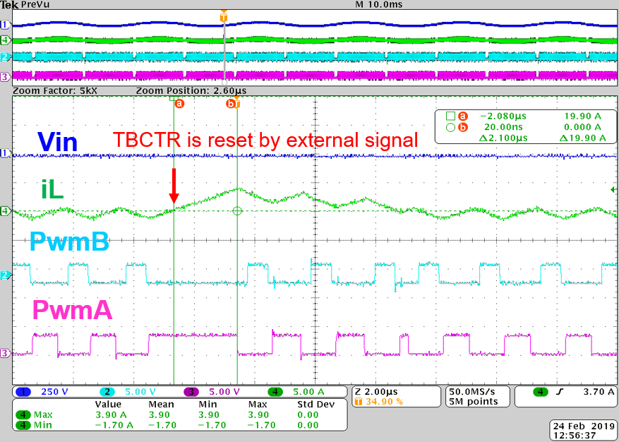
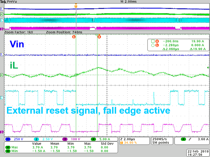
In my code, the EPWM7 output is updated based on the sensing signal and real-time calculation of the duty cycle in one interrupt. As shown in the following picture, the PWM output is occasionally all high in A and all low in B in one switching cycle, looking like a glitch or bug. i used complementary mode in PWM generation. And such glitch occurs in very low frequency (sometimes it takes ten seconds to capture one glitch). The sensed external signal and real-time calculation should be all right. Since my sampling frequency is 50kHz, and switching frequency is averagely 300kHz, if something wrong with the calculation and sensing signal, the PWM glitch will last for several switching cycles instead of only one cycle and occurs in so low frequency. so it looks more like a PWM glitch when updating the duty cycle.
I wonder, what will cause the EPWM module glitch or bug like this? How can i avoid such phenomenon?
By the way, the initialization function of the PWM is shown below. Values for EPWM_TIMER_TBPRD, EPWM_CMPA, EPWM_CMPB, EPWM_TIMER_PHASE, RED and FED are updated based on the calculation in one ADC interrupt.
// code/////////////
void InitEPwm7()
{
// Setup TBCLK
EPwm7Regs.TBCTL.bit.CTRMODE = TB_COUNT_UP; // Count up
EPwm7Regs.TBPRD = EPWM_TIMER_TBPRD; // Set timer period
EPwm7Regs.TBCTL.bit.PHSEN = TB_ENABLE; // Enable phase loading
EPwm7Regs.TBPHS.bit.TBPHS =0x0000; // Phase is 0
EPwm7Regs.TBCTL.bit.PRDLD = TB_SHADOW; //
EPwm7Regs.TBCTL2.bit.SYNCOSELX=1; //extended selection for sync out, EPWMxSYNCO = CMPC
EPwm7Regs.TBCTL.bit.SYNCOSEL = 3; //0:Sync Output Select is sync signal;1: when TB counter = zero; 3: extended,
EPwm7Regs.TBCTL.bit.HSPCLKDIV = TB_DIV1; // Clock ratio to SYSCLKOUT
EPwm7Regs.TBCTL.bit.CLKDIV = TB_DIV1;
//
// Setup shadow register load on ZERO
EPwm7Regs.CMPCTL.bit.SHDWAMODE = CC_SHADOW;
EPwm7Regs.CMPCTL.bit.SHDWBMODE = CC_SHADOW;
EPwm7Regs.CMPCTL.bit.LOADAMODE = CC_CTR_ZERO;
EPwm7Regs.CMPCTL.bit.LOADBMODE = CC_CTR_ZERO;
EPwm7Regs.CMPCTL2.bit.SHDWCMODE = CC_SHADOW;
EPwm7Regs.CMPCTL2.bit.LOADCMODE = CC_CTR_ZERO;
//
// Set Compare values
EPwm7Regs.CMPA.bit.CMPA = EPWM_CMPA; // Set compare A value
EPwm7Regs.CMPB.bit.CMPB = EPWM_CMPB; // Set Compare B value
EPwm7Regs.CMPC = EPWM_TIMER_PHASE; // 0.5 Ts
//
// Set actions on outputA, EPWM7A is the original PWM for SR switch
EPwm7Regs.AQCTLA.bit.CAU = AQ_SET; // Set PWM1A on event A, up count
EPwm7Regs.AQCTLA.bit.CBU = AQ_CLEAR; // Clear PWM1A on event B, up count
//
// Set Dead-Band Generator
EPwm7Regs.DBCTL.bit.IN_MODE = DBA_ALL; //EPWMA is the source for both falling edge and rising edge
EPwm7Regs.DBCTL.bit.OUT_MODE = DB_FULL_ENABLE; // enable dead-band module, bothFED and RED are active
EPwm7Regs.DBCTL.bit.POLSEL = DB_ACTV_HIC; // Active high complementary
EPwm7Regs.DBRED.bit.DBRED = RED; // set dead time before turning on SR switch
EPwm7Regs.DBFED.bit.DBFED= FED; // set dead time before turning on AC switch, Tr
// turn off gate signals when Vo over voltage through trip 1
EALLOW;
EPwm7Regs.TZSEL.bit.OSHT1 = 1; // enable T1 as the trigger signal
EPwm7Regs.TZCTL.bit.TZA = 2; // force EPWM7A to be LOW
EPwm7Regs.TZCTL.bit.TZB = 2; // force EPWM7B to be LOW
EDIS;
// turn off gate signals when over current through trip 2
EALLOW;
EPwm7Regs.TZSEL.bit.OSHT2 = 1; // enable T2 as the trigger signal
EPwm7Regs.TZCTL.bit.TZA = 2; // force EPWM7A to be LOW
EPwm7Regs.TZCTL.bit.TZB = 2; // force EPWM7B to be LOW
EDIS;
// turn off gate signals when over current through trip 3
EALLOW;
EPwm7Regs.TZSEL.bit.OSHT3 = 1; // enable T3 as the trigger signal
EPwm7Regs.TZCTL.bit.TZA = 2; // force EPWM7A to be LOW
EPwm7Regs.TZCTL.bit.TZB = 2; // force EPWM7B to be LOW
EDIS;
}
I really appreciate it if you could give me any hint or suggestions. This problem is really critical for my whole experiment.
Looking forward to your reply.


