Part Number: TMS320F28027
Other Parts Discussed in Thread: CONTROLSUITE, UNIFLASH
Tool/software: Code Composer Studio
Dear Ti community
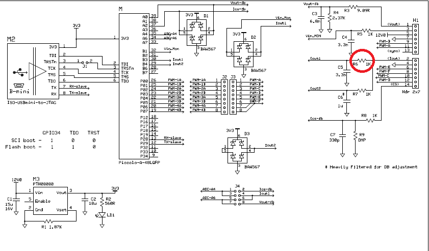
I'm developing PCMC on HVPSFB.
And I want to operate HVPSFB development_kits.
I supply 12V at TP1 at base board, remove R6 resister and J1 at controller card.
Then connect the USD cable attached the kit.
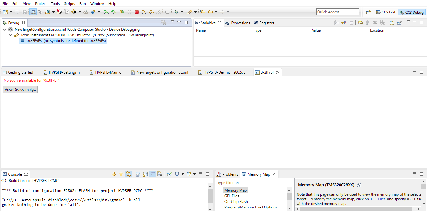
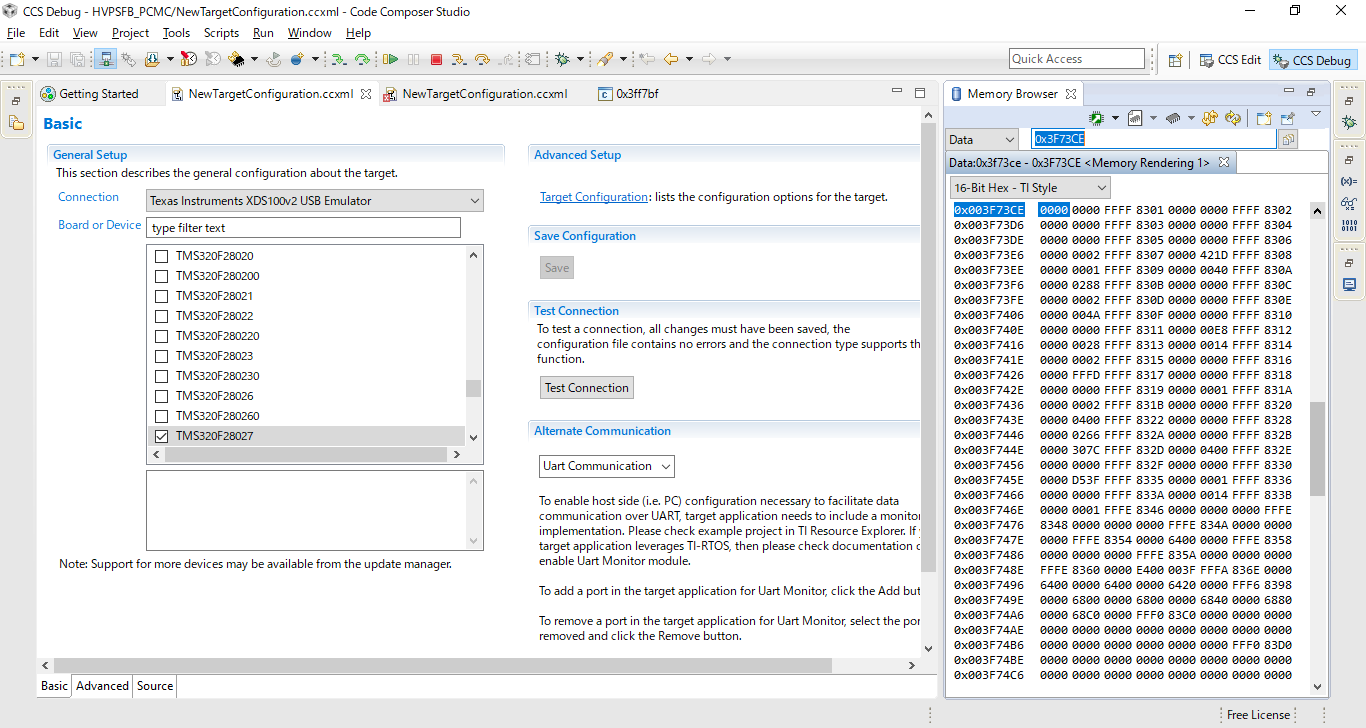
In CCS,create target configuration file and debug default HVPSFB_PCMC Project.
The debug success.
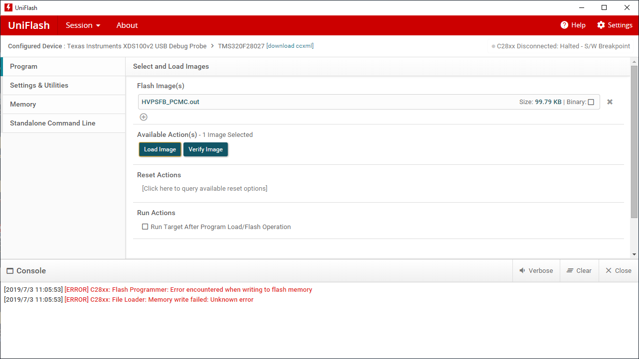
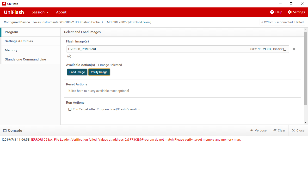
After that,I want to change the program.
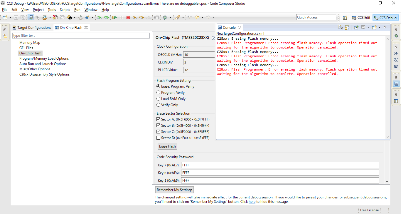
I debug same process,but the error occuer.
the error is
C28xx:error connecting to the target:(Error - 1135 @ 0x0)
the emulator reported an error.Confirm emulator configuration and connection,
reset the emulator,and retry the operation.
(Emulation package 5.1.507.0)
I tried R6,J1 populate,but same error occuer.
What is the cause?