This thread has been locked.

If you have a related question, please click the "Ask a related question" button in the top right corner. The newly created question will be automatically linked to this question.

LAUNCHXL-F28379D: Problem using ADCD module on the development board

Part Number: LAUNCHXL-F28379D

Hello all;

I'm trying to set up the ADCD on my LAUNCHXL-F28379D, I've been seeing the adc_ex1_soc_software project example for this board using Driverlib and just CPU1, this example uses just ADCA and ADCB. However, I want to use ADCD to take advantage of the differential features that this board has.

Where I'm stuck is in the ADC SOC configuration, the example uses the function

ADC_setupSOC(ADCA_BASE, ADC_SOC_NUMBER0, ADC_TRIGGER_SW_ONLY, ADC_CH_ADCIN0, 15); 

to set up the SOC, so I just tried to modify the function to work with the ADCD (ADCCLK is at 25 MHz) this is my version of this function 

ADC_setupSOC(ADCD_BASE, ADC_SOC_NUMBER0, ADC_TRIGGER_SW_ONLY, ADC_CH_ADCIN0_ADCIN1, 250);

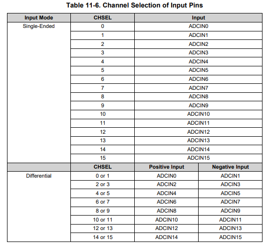
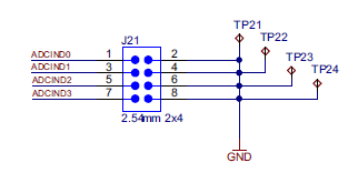
However, if you look at the 3rd variable (the bold one) that I'm giving to the function, it basically says that it will use as differential pins ADCIN0-ADCIN1 (in fact, the adc.h says as a comment "//!< differential, ADCIN0 and ADCIN1"), when what I want is something like ADCIND0 (as a subtraction with its matching pin) to take advantage of the J21 jumpers (according to the schematics, these jumpers deals with ADCIND0 to ADCIND3).

When I opened the adc.h it just allows to place values like ADCINx-ADCINy no ADCINDx-ADCINDy or similar is shown, so I think that maybe these ADCINx internally can be configured as ADCINDx but I cannot found where.

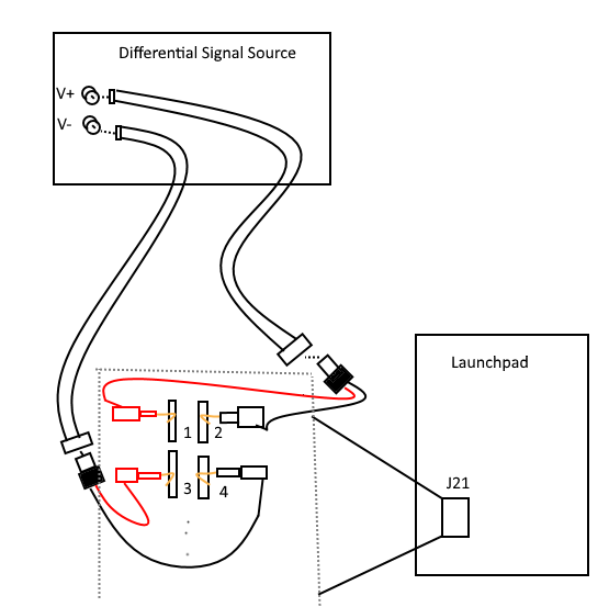
So, the question is: How can I set up the LAUNCHXL to read my analog differential signals from J21 pins?

  • Hi Kevin,

    To set the ADC in differential mode you need to use the ADC set mode function to configure the signal mode and resolution.  This is a global ADC setting; it can't be configured per SOC.  

    For the channel selects, if you look at the TRM, you can see that CH = 0 or CH = 1 is equivalent to CH = 0&1.

  • Hi Devin, thanks for your answer, however my doubts remain.

    If you take a look at the piece of code that I have right now (see the paragraph below), you'll be able to see that I've already settled what you told, however, what I don't understand is how can I configure, for example, if I place CHSEL = 9 as the ADCIND0 as the positive input and the pin aside as the negative input (see J21 pins).

    void ADC_Configure(void)
    {

    /* Actually the SYSCLK (ADCCLK feeder) is working at 200 MHz (see
    * variable DEVICE_SYSCLK_FREQ on device.h file) so dividing the
    * SYSCLK by 4 will make the ADC work at its upper limit (see
    * datasheet section "ADC Electrical Data and Timing", on table
    * "ADC Operating Conditions (16-Bit Differential Mode)", which is
    * 50 MHz, lower limit for ADCCLK is 5 MHz, due to this ADCCLK will
    * be used with a higher prescale. In this case 8 will be used to
    * get an ADCCLK = 25 MHz.
    * The datasheet indicates that power-up time is maximum 500 us, however
    * 1000 us are being used to ensure proper power-up and configuration */
    ADC_setPrescaler(ADCD_BASE, ADC_CLK_DIV_8_0);
    ADC_setMode(ADCD_BASE, ADC_RESOLUTION_16BIT, ADC_MODE_DIFFERENTIAL);
    ADC_setInterruptPulseMode(ADCD_BASE, ADC_PULSE_END_OF_CONV);
    ADC_enableConverter(ADCD_BASE);
    DEVICE_DELAY_US(1000);


    /* According to the datasheet, the minimum sample window duration is
    * 320 ns, which is 3.125 MHz (64 cycles of SYSCLK at 200 MHz), meaning
    * that this frequency cannot be exceeded. Also, according to the datasheet,
    * the 16-bit ADC requires between 29.6 and 31 ADCCLK cycles to interpret
    * the analog value that is being read by the MCU.
    * Because the ADCCLK was configured at 25 MHz, 31 ADCCLK cycles are about
    * 806.5 kHz, it will be rounded to 800 kHz to give the converter a bit more
    * of time to process the measurement, this takes us to 250 SYSCLK cycles needed
    * to give the ADCD a window wide enough to convert the data */
    ADC_setupSOC(ADCD_BASE, ADC_SOC_NUMBER0, ADC_TRIGGER_SW_ONLY,
    ADC_CH_ADCIN0_ADCIN1, 250);
    ADC_setupSOC(ADCD_BASE, ADC_SOC_NUMBER1, ADC_TRIGGER_SW_ONLY,
    ADC_CH_ADCIN2_ADCIN3, 250);
    ADC_setupSOC(ADCD_BASE, ADC_SOC_NUMBER2, ADC_TRIGGER_SW_ONLY,
    ADC_CH_ADCIN4_ADCIN5, 250);
    ADC_setupSOC(ADCD_BASE, ADC_SOC_NUMBER3, ADC_TRIGGER_SW_ONLY,
    ADC_CH_ADCIN6_ADCIN7, 250);

    }

  • Hi Kevin,

    Sorry, looks like I missed your key question in the original post.

    Only the differential combinations listed in the table above from the TRM are possible.  The silicon does not support something like D0 and D3 as a differential pair, only (D0 and D1) or (D2 and D3).

    You'll have to work around the available pins and pin topology in your particular EVM. We understand that this is not optimal. In your end application, you can layout the channels however you want, which should allow nicely differentially routed channel pairs.        

  • Ok, got it, I think you have my key question right now, but focused differently.

    If you take a look at the Users Guide for the LAUNCHXL, you'll realize that externally the only pins that I can take are some of the ADCINAx, ADCINBx, ADCINCx, and ADCINDx (these last ones from the J21 pinout set), you are not able to take from ADCIN0 to ADCIN13 (reason why I think that in some way these ADCINx are configured internally or by software in some way to be these ADCINDx that I need), EXCEPT for ADCIN14 and ADCIN15 that are directly mapped to the pinout J3 and J7, respectively.

    So, in terms that I want to use the J21 pinout set (the pinout that has already mapped 8 pins dedicated to ADCD inputs) that the LAUNCHXL already has available for me to take them on the board:

    1. How can I configure the ADC to work with these pins (that is, working with ADCD pins from ADCIND0 to ADCIND3)?

    2. When everything is set to work with J21 differential pins, the input for the analog to digital conversion for the first differential measurement will be the subtraction between pin 1 and pin 2, or will be the subtraction of pin 1 and pin 3 (meaning that pins 2, 4, 6 and 8 have nothing to do, for my understanding)? Please see the picture below to understand this last question.

  • I think I'm getting there. If I put:

    ADC_setPrescaler(ADCD_BASE, ADC_CLK_DIV_8_0);

    ADC_setMode(ADCD_BASE, ADC_RESOLUTION_16BIT, ADC_MODE_DIFFERENTIAL);

    ADC_setInterruptPulseMode(ADCD_BASE, ADC_PULSE_END_OF_CONV);

    ADC_enableConverter(ADCD_BASE);

    DEVICE_DELAY_US(1000);

    ADC_setupSOC(ADCD_BASE, ADC_SOC_NUMBER0, ADC_TRIGGER_SW_ONLY, ADC_CH_ADCIN0_ADCIN1, 250);

    From the setMode I'm telling the MCU that I'll use the ADCD as differential with 16 bits resolution, also, when I use the setupSOC, from the first argument of the function I'm telling the MCU that I'll use the ADCD, and from the 4th argument I'm telling it that I'll use the channel 0 of the ADCD (according to the table that you sent me, sending ADC_CH_ADCIN0_ADCIN1ADC_CH_ADCIN0 or ADC_CH_ADCIN1 results in the same thing -> first internal conversion), right? So, for me the channel 0 of the ADCD is the ADCIND0, is this correct? If so, I think my issue is now clear.

    Now the only doubt that I have is if the differential result for the first ADCD input channel will be the subtraction of pin 1 and 2 or pin 1 and 3 (according to J21 pinout). This is a doubt that came up to me from one of your replies, when you told me "The silicon does not support something like D0 and D3 as a differential pair, only (D0 and D1) or (D2 and D3)", if you take a look at the ADCIND0 and ADCIND1 these are the pins 1 and 3, so this means that the input for the differential conversion will be ADCIND0-ADCIND1 (pin1 - pin3)? I think the right way is (result0 = pin1 - pin2), result1 = (pin3 - pin4) and so on.

  • Hi Kevin,

    Pins 2,4,6,8 are all connected to ground.  The idea here would be to give you a place to clip your differential signal ground connections (although you'd probably want to twist your two cables together):

    You might also want to check out the datasheet diagram "Differential Signaling Mode" as well as this presentation:  

    The differential inputs on this device are 'fully differential' per the above presentation.  

  • Great, I totally understood this. Finally, if I put 

    ADC_setupSOC(ADCD_BASE, ADC_SOC_NUMBER0, ADC_TRIGGER_SW_ONLY, ADC_CH_ADCIN0_ADCIN1, 250);

    Am I telling the ADC to get as ADCD first conversion result0 = (ADCIND0 - ADCIND1), right?

  • Hi Kevin,

    Yes, that is correct. Do note that the difference can't be between arbitrary voltages ('true differential') but instead is the difference between two signals reflected about the common mode voltage ('fully differential'). The common mode voltage should always be near VREFHI/2.