This thread has been locked.

If you have a related question, please click the "Ask a related question" button in the top right corner. The newly created question will be automatically linked to this question.

TMS320F280049: Problem implementing SPI. Seeing loopback data when loopback is disabled.

Part Number: TMS320F280049
Other Parts Discussed in Thread: C2000WARE

Hello,

I'm having problems utilizing the driverlib SPI on the TMS320F280049 processor to communicate with an external serial NOR flash memory. I'm seeing data written returned with the same data shifted left by 8 bits even though I have disabled loopback. Can anyone help me identify what could be going wrong here?

My settings utilize the SCI-B interface

#define SPI_SIMO_PIN 56
#define SPI_SOMI_PIN 57
#define SPI_CLOCK_PIN 32
#define SPI_ENABLE_PIN 27

With all the pins configured as necessary for SPI use.

Baud rate set to LSPCLK frequency /4.

Bit rate set to 500000.

Data length set to 8.

SPI set to rising edge without delay, SPI_PROT_POLOPHA0.

Set to master mode.

Note, I don't use the FIFO, have the loopback disabled, and set the emulation mode to free run.

Highspeed and DMA are not used.

My SPI setup function calls

1) SPI_disableModule

2) SPI_setConfig

3) SPI_disableLoopback

4) SPI_setEmulationMode

5) then SPI_enableModule

My SPI transmission function:

1) Turns on the chip select (pin low)

2) Loops through the data message. SPI_writeDataNonBlocking then SPI_readDataBlockingNonFIFO until data is sent/readback.

3) Turns off the chip select (pin high)

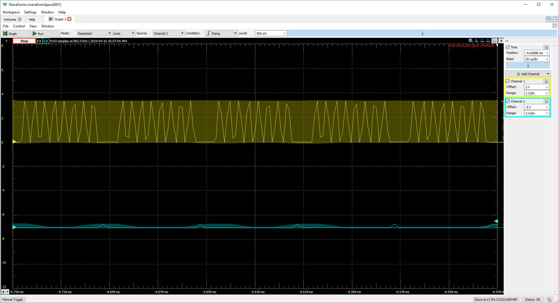
My test includes sending a message to read the manufacturer's ID using this message

uint16_t outIdData[20] =

{0x9F, 0x00, 0x00, 0x00,
 0x00, 0x00, 0x00, 0x00,
 0x00, 0x00, 0x00, 0x00,
 0x00, 0x00, 0x00, 0x00,
 0x00, 0x00, 0x00, 0x00};

This is what I see returned (as seen in watch):

inIdData unsigned int[20] [0x9FFF,0x00FF,0x00FF,0x00FF,0x00FF...] (Hex) 0x0000B028@Data
[0] unsigned int 0x9FFF (Hex) 0x0000B028@Data
[1] unsigned int 0x00FF (Hex) 0x0000B029@Data
[2] unsigned int 0x00FF (Hex) 0x0000B02A@Data
[3] unsigned int 0x00FF (Hex) 0x0000B02B@Data
[4] unsigned int 0x00FF (Hex) 0x0000B02C@Data
[5] unsigned int 0x00FF (Hex) 0x0000B02D@Data
[6] unsigned int 0x00FF (Hex) 0x0000B02E@Data
[7] unsigned int 0x00FF (Hex) 0x0000B02F@Data
[8] unsigned int 0x00FF (Hex) 0x0000B030@Data
[9] unsigned int 0x00FF (Hex) 0x0000B031@Data
[10] unsigned int 0x00FF (Hex) 0x0000B032@Data
[11] unsigned int 0x00FF (Hex) 0x0000B033@Data
[12] unsigned int 0x00FF (Hex) 0x0000B034@Data
[13] unsigned int 0x00FF (Hex) 0x0000B035@Data
[14] unsigned int 0x00FF (Hex) 0x0000B036@Data
[15] unsigned int 0x00FF (Hex) 0x0000B037@Data
[16] unsigned int 0x00FF (Hex) 0x0000B038@Data
[17] unsigned int 0x00FF (Hex) 0x0000B039@Data
[18] unsigned int 0x00FF (Hex) 0x0000B03A@Data
[19] unsigned int 0x00FF (Hex) 0x0000B03B@Data

Here is the SPIB register values:

SPICCR 0x0087 SPI Configuration Control Register [Memory Mapped]
SPICTL 0x0006 SPI Operation Control Register [Memory Mapped]
SPISTS 0x0000 SPI Status Register [Memory Mapped]
SPIBRR 0x000B SPI Baud Rate Register [Memory Mapped]
SPIRXEMU 0x00FF SPI Emulation Buffer Register [Memory Mapped]
SPIRXBUF 0x00FF SPI Serial Input Buffer Register [Memory Mapped]
SPITXBUF 0x0000 SPI Serial Output Buffer Register [Memory Mapped]
SPIDAT 0x00FF SPI Serial Data Register [Memory Mapped]
SPIFFTX 0xA000 SPI FIFO Transmit Register [Memory Mapped]
SPIFFRX 0x201F SPI FIFO Receive Register [Memory Mapped]
SPIFFCT 0x0000 SPI FIFO Control Register [Memory Mapped]
SPIPRI 0x0010 SPI Priority Control Register [Memory Mapped]

Thanks in advance,

-Wes

  • Wesley,

    I don't think that you are having a loopback like you expect. Have you observed your transmit and receive data lines on a scope? I suspect that you are actually just transmitting 0s because you are not left-shifting your transmit data. Also, I suspect that the SPISOMI line is held high, so you are just receiving 8 bits of 1s.

    What I think is happening:
    1. The Slave is actually not ever transmitting data back to the master so the SPISOMI pin is held high. Please verify.
    2. Transmitter is not left shifting the transmit data in the TX buffer. See the following transmission assuming SPISOMI is held high:
    a. SPI1 TX 0x009F, RX 0x9F00
    b. SPI2 TX 0x0000, RX 0x00FF
    c. SPI3 TX 0x0000, RX 0x00FF
    This is telling me that your transmit is only sending 8 bits (as configured), SPISOMI is held high and not receiving data from the slave. Since the transmit data Is not left shifted, it will transmit only the upper 8 bits of the transmit buffer (all 0s in your case)
    3. I'm guessing that you are only transmitting 0s always. Please verify this.

    This is the most likely scenario in my brief check.

    Regards,
    Mark
  • Hi Mark,

    Thanks for your input!

    1) This does appear to be the case. I'm seeing SPISOMI held high.

    2) This is the case. I must have glazed over the 'Data must be left-justified when written...' line in the SPI section of the technical reference document.

    3) This does appear to be the case. SPISIMO line is not showing data as I would expect.

    So after adjusting for left-justification of the data to be written, I am now seeing all 0x00FF values returned.

    I've checked the clock signal which appears to be running fine.

    The chip select pin appears to be acting as I expect it, driving low when sending and then high when not.

    But the SPISIMO appears to still be showing no values. I'll provide further data soon.

  • Here's an update after adding the left shift. 

    Even though the data is now correctly left-shifted, I'm still seeing 0s on the SPI SIMO line.

    Core code of transmit function:

            // Turn on specific device selection
            masterChipSelectOn(settings, deviceId);
    
            // Iterate over writeData and readData
            for (x = 0; x < dataCount; ++x)
            {
                // Data needs to be left shifted if not taking full 16 bits
                writeData[x] = writeData[x] << leftShift;
    
                // Write from writeData[x] to SPI device
                SPI_writeDataNonBlocking(settings->hardwareAddress, writeData[x]);
    
                // Read returned data into readData[x] from SPI device
                readData[x] = SPI_readDataBlockingNonFIFO(settings->hardwareAddress);
            }
    
            // Turn off specific device selection
            masterChipSelectOff(settings, deviceId);

    Note:

    'settings' is a structure with values to abstract the SPI device.

    settings->hardwareAddress = 0x00006110

    'writeData' is an input array pointer to the function

    'readData' is an output array pointer for the function

    The calling function uses the outIdData (writeData) and inIdData (readData) arrays.

    SIMO pin setup

    // Setup the SPI SIMO pin
    GPIO_setMasterCore(settings->simoPin, GPIO_CORE_CPU1);
    GPIO_setPadConfig(settings->simoPin, GPIO_PIN_TYPE_PULLUP);
    GPIO_setPinConfig(settings->simoPinConfig);
    GPIO_setQualificationMode(settings->simoPin, GPIO_QUAL_ASYNC);

    GPIO_setDirectionMode(settings->simoPin, GPIO_DIR_MODE_OUT);

    Note:

    settings->simoPin = 56

    settings->simoPinConfig =  0x00481009 (GPIO_56_SPISIMOB)

    Latest testing data:

    outIdData unsigned int[20] [0,0,0,0,0...] 0x0000040C@Data
    [0] unsigned int 0 0x0000040C@Data
    [1] unsigned int 0 0x0000040D@Data
    [2] unsigned int 0 0x0000040E@Data
    [3] unsigned int 0 0x0000040F@Data
    [4] unsigned int 0 0x00000410@Data
    [5] unsigned int 0 0x00000411@Data
    [6] unsigned int 0 0x00000412@Data
    [7] unsigned int 0 0x00000413@Data
    [8] unsigned int 0 0x00000414@Data
    [9] unsigned int 0 0x00000415@Data
    [10] unsigned int 0 0x00000416@Data
    [11] unsigned int 0 0x00000417@Data
    [12] unsigned int 0 0x00000418@Data
    [13] unsigned int 0 0x00000419@Data
    [14] unsigned int 0 0x0000041A@Data
    [15] unsigned int 0 0x0000041B@Data
    [16] unsigned int 0 0x0000041C@Data
    [17] unsigned int 0 0x0000041D@Data
    [18] unsigned int 0 0x0000041E@Data
    [19] unsigned int 0 0x0000041F@Data

    inIdData unsigned int[20] [0x00FF,0x00FF,0x00FF,0x00FF,0x00FF...] (Hex) 0x00000420@Data
    [0] unsigned int 0x00FF (Hex) 0x00000420@Data
    [1] unsigned int 0x00FF (Hex) 0x00000421@Data
    [2] unsigned int 0x00FF (Hex) 0x00000422@Data
    [3] unsigned int 0x00FF (Hex) 0x00000423@Data
    [4] unsigned int 0x00FF (Hex) 0x00000424@Data
    [5] unsigned int 0x00FF (Hex) 0x00000425@Data
    [6] unsigned int 0x00FF (Hex) 0x00000426@Data
    [7] unsigned int 0x00FF (Hex) 0x00000427@Data
    [8] unsigned int 0x00FF (Hex) 0x00000428@Data
    [9] unsigned int 0x00FF (Hex) 0x00000429@Data
    [10] unsigned int 0x00FF (Hex) 0x0000042A@Data
    [11] unsigned int 0x00FF (Hex) 0x0000042B@Data
    [12] unsigned int 0x00FF (Hex) 0x0000042C@Data
    [13] unsigned int 0x00FF (Hex) 0x0000042D@Data
    [14] unsigned int 0x00FF (Hex) 0x0000042E@Data
    [15] unsigned int 0x00FF (Hex) 0x0000042F@Data
    [16] unsigned int 0x00FF (Hex) 0x00000430@Data
    [17] unsigned int 0x00FF (Hex) 0x00000431@Data
    [18] unsigned int 0x00FF (Hex) 0x00000432@Data
    [19] unsigned int 0x00FF (Hex) 0x00000433@Data

    Some Scope captures (note, not the best scope)

    The following image shows channel 1 as the clock and channel 2 as the chip enable

    Note, enable signal is low when transmitting.

    The following image shows channel 1 again as the clock and channel 2 now as the SIMO pin.

  • Hi Wesley,

    It may be time to break down the problem.

    I noticed that a lot of your data is expected to be 0s. can you disconnect the Slave for now and focus on ensuring that the SPISIMO data is correctly being output? You can turn on internal loopback, or you can just transmit an expected data pattern to an unconnected pin, and observe on a scope.

    You shared the state of outIdData and it all appears to be 0s... so that is telling me that you are trying to transmit 0s, which is exactly what the SPI is doing. Did you add a left shift when writing to outIdData, and then left shift it again when you write it to the SPI transmit buffer?

    I am currently working with a SPI DAC and am doing the almost exactly the same thing. The c2000ware spi_ex4_eeprom example also has similar architecture.

    -Mark
  • Hi Mark,

    Mark Labbato said:

    I noticed that a lot of your data is expected to be 0s. can you disconnect the Slave for now and focus on ensuring that the SPISIMO data is correctly being output? You can turn on internal loopback, or you can just transmit an expected data pattern to an unconnected pin, and observe on a scope.

    I did this. I have a F280049 controlCard with docking station and modified the spi_ex5_external_loopback_fifo_interrupts project so that it utilizes my codebase. 

    Mark Labbato said:

    You shared the state of outIdData and it all appears to be 0s... so that is telling me that you are trying to transmit 0s, which is exactly what the SPI is doing. Did you add a left shift when writing to outIdData, and then left shift it again when you write it to the SPI transmit buffer?

    Wow. Good point. I overlooked this. This is now occurring because of the left shift correction. Since I was modifying the origin outIdData, I was left shifting the command out of existence.

    I fixed this issue now. I am seeing the expected data on the scope for SPISIMO, but my SPISOMI looks odd coming back from my external flash.

    Do you have any thoughts on what might be causing this? At any rate, I think that my logic is sound now, but I am unsure if a setting is perhaps causing this. 

    Here is an image showing Channel 1 Clock and Channel 2 SPISIMO.

    Here is an image showing Channel 1 SPISOMI and Channel 2 SPISIMO.

    Here is an image showing Channel 1 SPISOMI and Channel 2 Clock

  • Here is a scope recording of the Channel 1 Select and Chanel 2 SPISIMO. Note, my code only toggles the select pin at the beginning and end of the transmission. The driverlib/hardware is toggling it as well?

  • Hi Mark,

    I changed the STE pin to be configured as a GPIO. This looks better to me/similar to previous designs' signals. Unfortunately, I'm still not seeing the data that I expect (flash ID data; 0x20, 0xBA, 0x20 on the SOMI line). At this point, I suspect a problem with my flash chip or some setting between the device and processor. If you have any thoughts on why I may not be seeing the expected data, I would appreciate hearing them, but I do think my original problem is fixed. Thanks for all your help!

    Channel 1 SOMI with Channel 2 SIMO

    Channel 1 SOMI with Channel 2 Clock

    Channel 1 Enable with Channel 2 SOMI (Enable showing Low as expected)

  • Sorry , been a busy day on my end as well. Glad you traced the original problem down.

    Yes if you want to use a manual chip select, you do NOT want that GPIO mux to be configured for the SPI. It should be GPIO output pin. You found out that if a pin is configured to a peripheral mux position, you can change the GPIO state, mode, direction, etc and it won't matter since the Peripheral is in control (except for input qualification).

    Regarding not getting expected data back from the Flash chip, check your polarity and phase settings. don't just go by "mode0" or "Polarity1/phase0". C2000 doesn't match up with all manufacturers as to what the Polarity0 means or Mode 1 means. Ensure that the transmit and RX latch edges match between them rather than the naming convention.

    Also, be sure to check your init packets to the slave device. did you transmit all of the proper commands? did you allow enough time between different commands. (e.g. wait 100ms after the init command to allow the flash device to init). Is your chip select meant to be held active during the full transfer you were originally stuck on? does it need to toggle between the command byte and the response packet?

    Ask yourself those types of questions while interfacing with new chips and you should be able to figure it out.

    -Mark
  • Thanks Mark! Much appreciated.