This thread has been locked.

If you have a related question, please click the "Ask a related question" button in the top right corner. The newly created question will be automatically linked to this question.

TMS320F28034: Check about 3.3V power on time

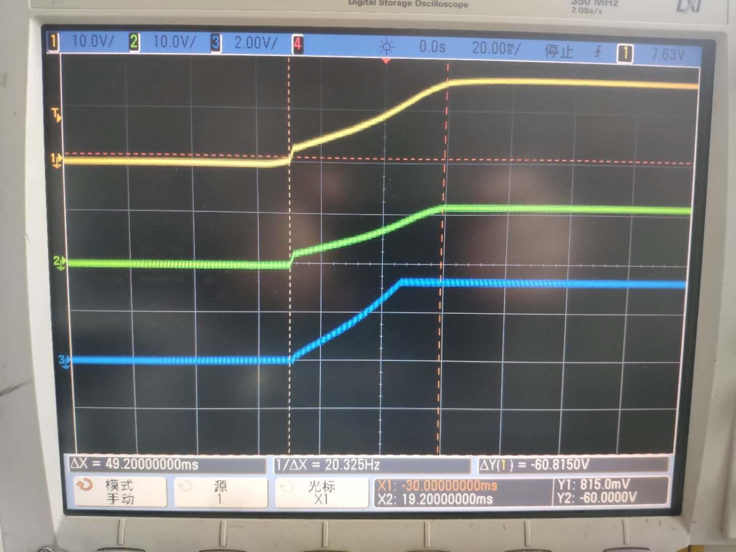
Part Number: TMS320F28034

Hi

What's the typical time of 3.3V power on?

As below blue curve, 3.3V power on time is 40mS.

Double check with you, is it OK?

  • Hi Daniel,

    There is no minimum ramp rate specified in the F2803x datasheet, so this should be OK.

    On newer devices (e.g. F2837x) we specify a minimum supply ramp rate of 330V/s, which equates to a requirement that the supply ramp fully in about 10ms.  

    Why is the ramp so slow?  

  • Daniel,

    There is some clarification here from us.  While there is not a specification in the datasheet for "supply ramp rate", there are some parameters that need to be observed to ensure that the device is in a proper state when XRSn is released by the internal POR/BOR logic.

    Key parameters:

    BOR minimum voltage trip point: 2.42V

    BOR min time to hold XRSn AFTER trip point is reached: 400us 

    http://www.ti.com/document-viewer/TMS320F28027/datasheet/electrical-characteristics-tsprs4398192004100431#tsprs4398192004100431

    Vmin of the device: 2.97V

    http://www.ti.com/document-viewer/TMS320F28027/datasheet/recommended-operating-conditions-tsprs517-83120041015401#tsprs517_83120041015401

    Summary:  

    Up to at least 2.42V the on-chip POR/BOR logic will hold the XRSn pin active low keeping the device in reset.  What is important is that by the time the module releases XRSn that the device VDDIO be within the operational range in the datasheet, which is 2.97V or greater.

    Using the parameters above this means that after we reach 2.42V we have 400us in which to be at 2.97V so that we are within specification.

    2.97V-2.42V = 0.55V       0.55V/400us = 1.375V/ms ramp rate

    If we assume the ramp rate to be linear from 0V to 3.3V(nom target) this means that the total ramp the customer is showing needs to occur in 2.4ms to avoid any potential issues.

    At this point the customer ramp is out of specification, it would only be ~2.5xxV at the min time specified for BOR release.

    Keep in mind that this is worst case, if the BOR limit is higher on a specific device or the XRSn release time is larger this will give more margin; but for production the worst case number needs to be used to ensure all devices behave properly.

    Finally, this assumes that the customer has no active voltage supervisor that is driving XRSn externally based on VDDIO and only relying on the internal logic for XRSn control.  If the customer is controlling XRSn the ramp rate could be longer so long as XRSn is not released before Vmin = 2.97V.

    Best,
    Matthew