


Part Number: TMS320F280049C
Other Parts Discussed in Thread: TMS320F28377D, , TMS320F280049
Hello,
Some info on our design first:
- We have connected a SPI peripheral of the TMS320F280049C to a McBSP peripheral of the TMS320F28377D used in clock-stop mode.
- The TMS320F28377D is the master and the TMS320F280049C is the slave.
- The link frequency is 20MHz.
- The transmission FIFO of the SPI peripheral of the TMS320F280049C is used.
- Due to a design error, the FSR signal of the McBSP peripheral is not used as the source of the chip select for the TMS320F280049, we use a GPIO instead which is set low after the init and kept low all the time.
- Both processor are configured to output data on the rising edge and sample data on the falling edge.
Now that I have given some insight on our design for better understanding, let's jump to the question.
During our tests, we are encoutering some transmissions issues.
The TMS320F28377D sends dummy data to push the data out of the TMS320F280049C which is expected to send the following data:
0xEEEE 0xDDDD 0xCCCC 0xBBBB 0xEDCB 0xA987 0x789A 0xBCDE 0xAAAA 0x9999 0x8888 0x7777 0x3501 0x2135 0x4141 0x3535
However, the data received successively in the TMS320F28377D are the following:
0xEEEF 0xBBBB 0x9999 0x7777 0xDB97 0x530E 0xF135 0x79BD 0x5555 0x3333 0x1110 0xEEEE 0x6A02 0x426A 0x8282 0x6A6A
We have analysed the output data and feel we understood what is happening.
Instead of 0xEEEE, we receive 0xEEEF and the following word is then equal to 0xBBBB instead of 0xDDDD.
So it seems the last bit of the first word is in fact the first bit of the second word as 0xBBBB corresponds to 0xDDDD shifted by 1 on the left and the msb of 0xDDDD is equal to 1.
We checked on all the following data and we confirm that behavior, for each word the last bit is equal to the first bit of the word which follows and after the first word from the FIFO all subsequent words are shifted by 1 on the left.
We captured with an oscilloscope the expected 0xEEEE word :

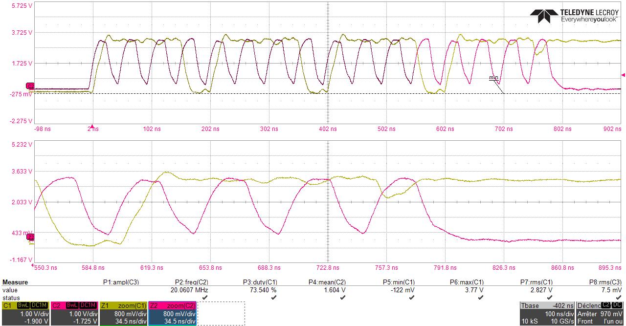
So you see on the screenshot that on the last bit, the TMS320F280049C tries to output the 0 but changes to 1 during the same clock rising edge, which confirms our analysis above.
However, I don't see any reason why it would behave like that, it seems the FIFO walks to the next word during the last bit transmission and leads to the bit change but that is not what we would expect to see.
The initialization code of the McBSP peripheral is the following:
void MCBSP_intializeLink(volatile struct McBSP_REGS *mcbsp)
{
    EALLOW;
    mcbsp->SPCR2.all        = 0;    // Reset FS generator, sample rate
                                    // generator & transmitter
    mcbsp->SPCR1.all        = 0;    // Reset Receiver, Right justify word
    mcbsp->SPCR2.bit.GRST   = 0;    // Reset the sample rate generator

    mcbsp->SPCR1.bit.CLKSTP = 2;    // Clock stop mode without clock delay
    mcbsp->PCR.bit.CLKXP    = 0;    // Transmit clock polarity bit (rising edge)
    mcbsp->PCR.bit.CLKRP    = 0;    // receive clock polarity bit (falling edge)
    mcbsp->RCR2.bit.RDATDLY = 1;    // RX data delay is 1 bit
    mcbsp->XCR2.bit.XDATDLY = 1;    // TX data delay is 1 bit
    mcbsp->PCR.bit.CLKXM    = 1;    // CLKX generated internally, CLKR derived from an external source
    mcbsp->PCR.bit.SCLKME   = 0;    // Sample rate generator input clock
    mcbsp->SRGR2.bit.CLKSM  = 1;    // is LSPCLK

#ifndef HWV2
    mcbsp->SRGR1.bit.CLKGDV = 222;  // Clock is 448 kHz.
#else
    mcbsp->SRGR1.bit.CLKGDV = 4;    // Clock is 20 MHz.
#endif

    mcbsp->PCR.bit.FSXM     = 1;    // FSX generated internally,
    mcbsp->PCR.bit.FSXP     = 1;    // FSX transmit pulse is active low
    mcbsp->SRGR2.bit.FSGM   = 0;    // Frame-synchronization pulses from the copying cotent of DXR

#ifndef HWV2
    mcbsp->RCR1.bit.RWDLEN1 = 4;    // Receive length 24 bits
    mcbsp->XCR1.bit.XWDLEN1 = 4;    // Transmit length 24 bits
#else
    mcbsp->RCR1.bit.RWDLEN1 = 2;    // Receive length 16 bits
    mcbsp->XCR1.bit.XWDLEN1 = 2;    // Transmit length 16 bits
#endif

    mcbsp->SPCR1.bit.RJUST  = 0;    // Data is rigth justified
    mcbsp->SPCR2.bit.FREE   = 1;    // Set FREE bit, Halting on a breakpoint will not halt the SPI
    mcbsp->SRGR2.bit.GSYNC  = 0;    // No clock sync for CLKG
    //
    // Enable Sample rate generator and
    // wait at least 2 CLKG clock cycles
    //
    mcbsp->SPCR2.bit.GRST   = 1;
    MCBSP_clkg_delay_loop();

    //
    // Release from reset
    // RX, TX and frame sync generator
    //
    mcbsp->SPCR2.bit.XRST   = 1;
    mcbsp->SPCR1.bit.RRST   = 1;
    MCBSP_clkg_delay_loop();

    mcbsp->SPCR2.bit.FRST   = 1;
    EDIS;
}
The initialization code of the SPI link is the following:
void SPI_initializeMainLink(volatile struct SPI_REGS *spi)
{
    spi->SPICCR.bit.SPISWRESET      = 0;       // Enter into SPI SWRESET mode

    /* Init FIFO */
    spi->SPIFFTX.bit.SPIRST         = 0;       //  SPI Reset
    spi->SPIFFTX.bit.SPIFFENA       = 1;       // FIFO Enhancements Enable
    spi->SPIFFTX.bit.TXFIFO         = 1;       // TXFIFO Reset
    spi->SPIFFTX.bit.TXFFINTCLR     = 1;       // TXFIFO Interrupt Clear
    spi->SPIFFTX.bit.TXFFIL         = 0x7 ;    // TXFIFO Interrupt Level
    spi->SPIFFRX.bit.RXFIFORESET    = 1;       // RXFIFO Reset
    spi->SPIFFRX.bit.RXFFINTCLR     = 1;       // RXFIFO Interrupt Clear
    spi->SPIFFRX.bit.RXFFIL         = 0x8 ;    // RXFIFO Interrupt Level

    spi->SPIFFCT.all                = 0x0;
    spi->SPICCR.bit.CLKPOLARITY     = 0 ;      // Clock polarity (0 == rising, 1 == falling)
    spi->SPICCR.bit.SPICHAR         = (16-1);  // 16-bit character
    spi->SPICTL.bit.MASTER_SLAVE    = 0;       // Enable master (0 == slave, 1 == master);
    spi->SPICTL.bit.TALK            = 1;       // Enable transmission (Talk)
    spi->SPICTL.bit.CLK_PHASE       = 0;       // Clock phase (0 == normal, 1 == delayed)
    spi->SPICTL.bit.SPIINTENA       = 0;       // SPI interrupts are disabled
    spi->SPIBRR.bit.SPI_BIT_RATE    = 4;       // Set the baud rate 4MHz for a 100MHz LSPCLK
    spi->SPIPRI.bit.TRIWIRE         = 0;       // Disable 3-wires
    spi->SPIPRI.bit.FREE            = 1;       // Set FREE bit, Halting on a breakpoint will not halt the SPI
    spi->SPIFFCT.bit.TXDLY          = 0;       // Transmit delay
    spi->SPIFFTX.bit.SPIRST         = 1;       //  SPI Reset

    spi->SPICCR.bit.SPISWRESET      = 1;       // Release the SPI from reset
}
I have tried to change the link frequency or tweak a bit the TXDLY on the SPI link without any luck.
Looking forward to your answer,
Clément

