Hi
My customer use 28377+ FPGA(spartan6) to extend 2pcs RAM(512K) and Flash(128K), double check with you about the hardware design and software change.
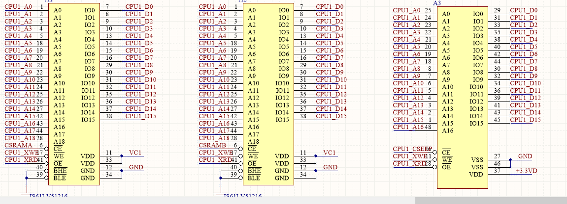
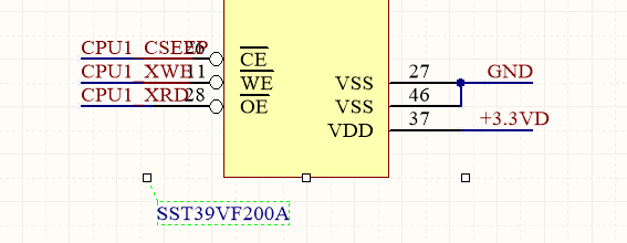
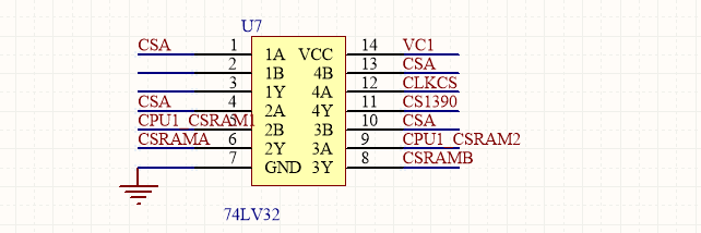
CPU1RAM is enabled by 74LV32
F28377
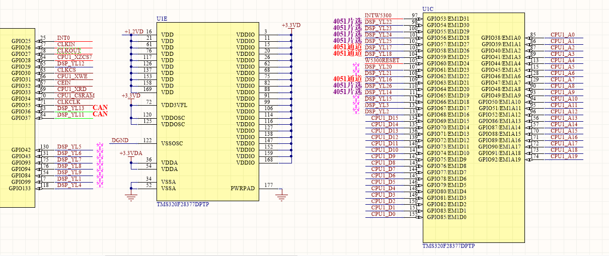
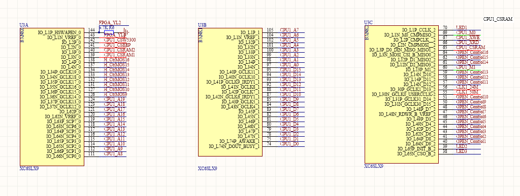
FPGA
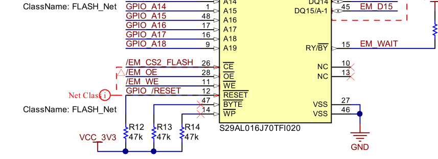
Use CS2 to extend RAM1 RAM2, CS4 is used to extend Flash, read and writing controlled by FPGA

Change example code as below
emif1_16bit_asram.c

Set IO to function 2 as expansion port
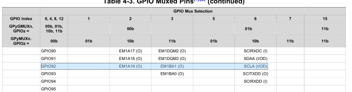
GPIO92 used for XA19, No changes in others code.
CCS7.4 MEMOREY observation
1. Write a 32-bit data, only the upper 16 bits have been written in, the address value will be cleared immediately when next statement is executed.
2. When writing to address 0x100002, the address line A0-A4 is 1000; How to configure XA19? is it necessary to set?
3. Emif1ConfigRegs.EMIF1MSEL.all = 0x93A5CE71; After write in, the read out data is 01?
Thanks a lot.