This thread has been locked.

If you have a related question, please click the "Ask a related question" button in the top right corner. The newly created question will be automatically linked to this question.

CCS/LAUNCHXL-F28027F: ADC - Normalize Data, and RANGE OF INPUT

Part Number: LAUNCHXL-F28027F
Other Parts Discussed in Thread: LAUNCHXL-F28027, CONTROLSUITE

Tool/software: Code Composer Studio

Dear TI members,

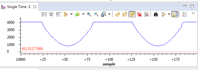
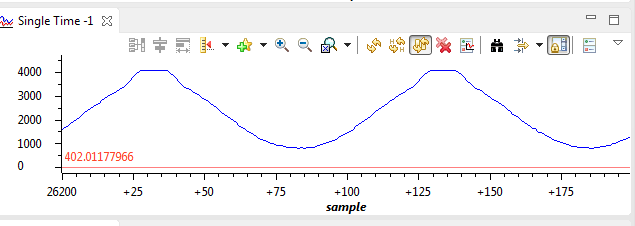
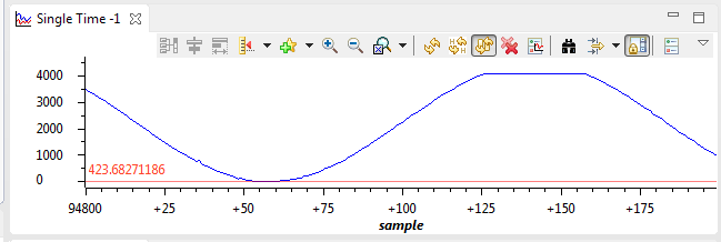
I come here to ask two question after struggling for several hours for a couple of days trying to solve this issue by myself. My LAUNCHXL-F28027 says it can handle an input of 0-3.3V, so I am trying to send a signal with Vpp = 3V and Voffset = +1.5V (connected between ADCINA1 and GND in my board), but when I do that, my ADC becomes saturated as if the signal input is going beyond its limitations. Figures of my ports and my ADC output are shown below. Since my ADC is 12bits, I expected that if I send a signal Vhigh = 3.3V and Vlow = 0V, my ADC.RESULT would give me values ranging between 0 and 4095...

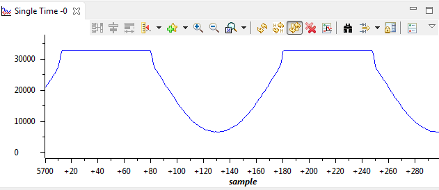
Besides the offset problem, I am also struggling with the simple task of adjusting this signal so that it can be sent to "spll1.AC_input" needed for the 1ph PLL function from Solar lib "SPLL_1ph_IQ_FUNC(&spll1);". Supposing that my ADC output signal is ranging from around 6600 to 24000 (when I send Vhigh = 1.5V and Vlow=0V), should I manually add a -15300 to set the signal to +- 8700, or is there a function from IQmath that does that?

I would really appreciate any help with these beginner questions since they are holding me from moving forward with my work.

Thank you,

Victor

  • Victor,
    Just to confirm I'm looking at the same SW, are you using the solar project located here (in control suite install)
    C:\ti\controlSUITE\development_kits\HV_SOLAR_DC_AC_v1.1\SolarHv_DCAC_PiccoloB_Rev_02\


    You are correct that the ADC range is 0-3.3V, assuming that the internal BG reference is used. If the source is the same as the above this is true.

    For the graph of the ADC output, can you look at the properties and determine which variable is being monitored and find in the code where that is calculated? I'd like to make sure that it is not the calculation that is saturating vs the ADC output saturating. Another way to do this would be to look at the ADC Result register that corresponds to this value and see if it is at 4095 as well.

    The above will help me determine the direction to take this debug.

    For your SPLL question, can you give me the file name where these variables/functions exist, and I can look at the IQ math transformation that is intended to comment further.

    Best,
    Matthew
  • Dear Matthew,

    I really appreciate your willingness to help. I compared my ADC with the one from the solar project you mentioned, and they seem to match. I have added my Adc.c below:

    /**********************************************************************
    * File: Adc.c
    **********************************************************************/
    
    #include "3ph_PLL_DEFINES.h"				// Main include file
    
    void InitAdc(void)
    {
    	asm(" EALLOW");						// Enable EALLOW protected register access
    
    	AdcRegs.ADCCTL1.bit.RESET = 1;		// Reset the ADC
    	asm(" NOP");
    	asm(" NOP");
    	
    //--- Power-up and configure the ADC
    	AdcRegs.ADCCTL1.all = 0x00E4;		// Power-up reference and main ADC
    // bit 15        0:      RESET, ADC software reset, 0=no effect, 1=resets the ADC
    // bit 14        0:      ADCENABLE, ADC enable, 0=disabled, 1=enabled
    // bit 13        0:      ADCBSY, ADC busy, read-only
    // bit 12-8      0's:    ADCBSYCHN, ADC busy channel, read-only
    // bit 7         1:      ADCPWDN, ADC power down, 0=powered down, 1=powered up
    // bit 6         1:      ADCBGPWD, ADC bandgap power down, 0=powered down, 1=powered up 
    // bit 5         1:      ADCREFPWD, ADC reference power down, 0=powered down, 1=powered up 
    // bit 4         0:      reserved
    // bit 3         0:      ADCREFSEL, ADC reference select, 0=internal, 1=external
    // bit 2         1:      INTPULSEPOS, INT pulse generation, 0=start of conversion, 1=end of conversion
    // bit 1         0:      VREFLOCONV, VREFLO convert, 0=VREFLO not connected, 1=VREFLO connected to B5
    // bit 0         0:      Must write as 0.
    
    	DelayUs(1000);						// Wait 1 ms after power-up before using the ADC
    
    //--- SOC0 configuration
    	AdcRegs.ADCSAMPLEMODE.bit.SIMULEN0 = 0;		// SOC0 in single sample mode (vs. simultaneous mode)
    												//if 1, SOC0 & SOC1 are simul
    	//trigger ADC
    	AdcRegs.ADCSOC0CTL.bit.TRIGSEL = 7;			// Trigger using ePWM2A
    	AdcRegs.ADCSOC1CTL.bit.TRIGSEL = 7;			//page  428. For now, ePWM is fine
    	//AdcRegs.ADCSOC2CTL.bit.TRIGSEL = 7;
    	//AdcRegs.ADCSOC3CTL.bit.TRIGSEL = 7;
    
    	//Sets ADC channels
    	AdcRegs.ADCSOC0CTL.bit.CHSEL = 1;			// Convert channel ADCINA1 (ch0)
    	AdcRegs.ADCSOC1CTL.bit.CHSEL = 3;			// Convert channel ADCINB1 (ch1)
    	//AdcRegs.ADCSOC2CTL.bit.CHSEL = 1;			// Convert channel ADCINA1 (ch2)
    	//AdcRegs.ADCSOC3CTL.bit.CHSEL = 9;			// Convert channel ADCINB1 (ch3)
    
    	//acquisition window duration
    	AdcRegs.ADCSOC0CTL.bit.ACQPS = 6;			// Acquisition window set to (6+1)=7 cycles = 333ns
    	AdcRegs.ADCSOC1CTL.bit.ACQPS = 6;
    	//AdcRegs.ADCSOC2CTL.bit.ACQPS = 6;
    	//AdcRegs.ADCSOC3CTL.bit.ACQPS = 6;
    
    	AdcRegs.ADCINTSOCSEL1.bit.SOC0 = 0;			// No ADCINT triggers SOC0.  TRIGSEL field determines trigger. (?)
    	AdcRegs.SOCPRICTL.bit.SOCPRIORITY = 0;		// All SOCs handled in round-robin mode
    
    //--- ADCINT1 configuration
    	AdcRegs.INTSEL1N2.bit.INT1CONT = 1;			// IF 0, ADCINT1 WAITS FOR FLAG TO BE CLEARED IN ISR. IF 1 ADCINT1 pulses regardless of ADCINT1 flag state
    	AdcRegs.INTSEL1N2.bit.INT1E = 1;			// Enable ADCINT1
    	AdcRegs.INTSEL1N2.bit.INT1SEL = 0;			// EOC0 triggers ADCINT1
    
    	PieCtrlRegs.PIEIER1.bit.INTx1 = 1;			// Enable ADCINT1 in PIE group 1
    	IER |= 0x0001;								// Enable INT1 in IER to enable PIE group
    
    //--- Finish up
    	AdcRegs.ADCCTL1.bit.ADCENABLE = 1;	// Enable the ADC
    	asm(" EDIS");						// Disable EALLOW protected register access
    
    } // end InitAdc()
    
    
    //--- end of file -----------------------------------------------------
    

    Here is the 1ph_PLL code that I have been using. I got it from C28x SolarLib v1.2 (Jan-14th):

    #include "Solar_IQ.h"
    
    //*********** Structure Init Function ****//
    void SPLL_1ph_IQ_init(int Grid_freq, long DELTA_T, SPLL_1ph_IQ *spll_obj)
    {
    	spll_obj->Upd[0]=SPLL_Q(0.0);
    	spll_obj->Upd[1]=SPLL_Q(0.0);
    	spll_obj->Upd[2]=SPLL_Q(0.0);
    	
    	spll_obj->ynotch[0]=SPLL_Q(0.0);
    	spll_obj->ynotch[1]=SPLL_Q(0.0);
    	spll_obj->ynotch[2]=SPLL_Q(0.0);
    	
    	spll_obj->ylf[0]=SPLL_Q(0.0);
    	spll_obj->ylf[1]=SPLL_Q(0.0);
    	
    	spll_obj->sin[0]=SPLL_Q(0.0);
    	spll_obj->sin[1]=SPLL_Q(0.0);
    	
    	spll_obj->cos[0]=SPLL_Q(0.999);
    	spll_obj->cos[1]=SPLL_Q(0.999);
    	
    	spll_obj->theta[0]=SPLL_Q(0.0);
    	spll_obj->theta[1]=SPLL_Q(0.0);
    	
    	spll_obj->wn=SPLL_Q(2*3.14*Grid_freq);
    
    	// loop filter coefficients for 20kHz
    	spll_obj->lpf_coeff.B0_lf=SPLL_Q(B0_LPF);
    	spll_obj->lpf_coeff.B1_lf=SPLL_Q(B1_LPF);
    	spll_obj->lpf_coeff.A1_lf=SPLL_Q(A1_LPF);
    	
    	spll_obj->delta_t=DELTA_T;  
    }
    
    //*********** Structure Coeff Update *****//
    void SPLL_1ph_IQ_notch_coeff_update(float delta_T, float wn,float c2, float c1, SPLL_1ph_IQ *spll_obj)
    {
    	// Note c2<<c1 for the notch to work
    	float x,y,z;
    	x=(float)(2.0*c2*wn*delta_T);
    	y=(float)(2.0*c1*wn*delta_T);
    	z=(float)(wn*delta_T*wn*delta_T);
    
    	spll_obj->notch_coeff.A1_notch=SPLL_Q(y-2);
    	spll_obj->notch_coeff.A2_notch=SPLL_Q(z-y+1);
    	spll_obj->notch_coeff.B0_notch=SPLL_Q(1.0);
    	spll_obj->notch_coeff.B1_notch=SPLL_Q(x-2);
    	spll_obj->notch_coeff.B2_notch=SPLL_Q(z-x+1);
    }
    	
    //*********** Function Definition ********//
    void SPLL_1ph_IQ_FUNC(SPLL_1ph_IQ *spll_obj)
    {
    	//-------------------//
    	// Phase Detect 	 //
    	//-------------------//
    	
    	spll_obj->Upd[0]=SPLL_Qmpy(spll_obj->AC_input,spll_obj->cos[1]);
    	
    	//-------------------//
    	//Notch filter structure//
    	//-------------------//
    	
    	spll_obj->ynotch[0]=-SPLL_Qmpy(spll_obj->notch_coeff.A1_notch,spll_obj->ynotch[1])-SPLL_Qmpy(spll_obj->notch_coeff.A2_notch,spll_obj->ynotch[2])+SPLL_Qmpy(spll_obj->notch_coeff.B0_notch,spll_obj->Upd[0])+SPLL_Qmpy(spll_obj->notch_coeff.B1_notch,spll_obj->Upd[1])+SPLL_Qmpy(spll_obj->notch_coeff.B2_notch,spll_obj->Upd[2]);
    	
    	// update the Upd array for future
    	spll_obj->Upd[2]=spll_obj->Upd[1];
    	spll_obj->Upd[1]=spll_obj->Upd[0];
    	
    	//---------------------------//
    	// PI loop filter 			 //
    	//---------------------------//
    	
    	spll_obj->ylf[0]=-SPLL_Qmpy(spll_obj->lpf_coeff.A1_lf,spll_obj->ylf[1])+SPLL_Qmpy(spll_obj->lpf_coeff.B0_lf,spll_obj->ynotch[0])+SPLL_Qmpy(spll_obj->lpf_coeff.B1_lf,spll_obj->ynotch[1]);
    	
    	//update array for future use
    	spll_obj->ynotch[2]=spll_obj->ynotch[1];
    	spll_obj->ynotch[1]=spll_obj->ynotch[0];
    	
    	spll_obj->ylf[1]=spll_obj->ylf[0];
    	
    	//------------------//
    	// VCO              //
    	//------------------//
    	
    	spll_obj->wo=spll_obj->wn+spll_obj->ylf[0];
    	
    	//integration process
    	spll_obj->sin[0]=spll_obj->sin[1]+SPLL_Qmpy((SPLL_Qmpy(spll_obj->delta_t,spll_obj->wo)),spll_obj->cos[1]);
    	spll_obj->cos[0]=spll_obj->cos[1]-SPLL_Qmpy((SPLL_Qmpy(spll_obj->delta_t,spll_obj->wo)),spll_obj->sin[1]);
    
    	if(spll_obj->sin[0]>SPLL_Q(0.99))
    		spll_obj->sin[0]=SPLL_Q(0.99);
    	else if(spll_obj->sin[0]<SPLL_Q(-0.99))
    		spll_obj->sin[0]=SPLL_Q(-0.99);
    	
    	if(spll_obj->cos[0]>SPLL_Q(0.99))
    		spll_obj->cos[0]=SPLL_Q(0.99);
    	else if(spll_obj->cos[0]<SPLL_Q(-0.99))
    		spll_obj->cos[0]=SPLL_Q(-0.99);
    	
    	spll_obj->theta[0]=spll_obj->theta[1]+SPLL_Qmpy(SPLL_Qmpy(spll_obj->wo,SPLL_Q(0.159154943)),spll_obj->delta_t);
    	
    	if(spll_obj->sin[0]>SPLL_Q(0.0) && spll_obj->sin[1]<=SPLL_Q(0.0))
    	{
    		spll_obj->theta[0]=SPLL_Q(0.0);
    	} 
    	
    	spll_obj->theta[1]=spll_obj->theta[0];
    	
    	spll_obj->sin[1]=spll_obj->sin[0];
    	spll_obj->cos[1]=spll_obj->cos[0];
    }


    Here is he 1ph_PLL.h:

    #ifndef SPLL_1ph_IQ_H_
    #define SPLL_1ph_IQ_H_
    
    #define SPLL_Q _IQ21
    #define SPLL_Qmpy _IQ21mpy
    
    //*********** Structure Definition ********//
    typedef struct{
    	int32	B2_notch;
    	int32	B1_notch;
    	int32	B0_notch;
    	int32	A2_notch;
    	int32	A1_notch;
    }SPLL_1ph_IQ_NOTCH_COEFF; 
    
    typedef struct{
    	int32	B1_lf;
    	int32	B0_lf;
    	int32	A1_lf;
    }SPLL_1ph_IQ_LPF_COEFF;
    
    typedef struct{
    	int32	AC_input;
    	int32	theta[2];
    	int32	cos[2];
    	int32	sin[2];
    	int32	wo;
    	int32	wn;
    	
    	SPLL_1ph_IQ_NOTCH_COEFF notch_coeff;
    	SPLL_1ph_IQ_LPF_COEFF	lpf_coeff;
    		
    	int32	Upd[3];
    	int32	ynotch[3];
    	int32	ylf[2];
    	int32	delta_t;
    }SPLL_1ph_IQ;
    
    //*********** Function Declarations *******//
    void SPLL_1ph_IQ_init(int Grid_freq, long DELTA_T, SPLL_1ph_IQ *spll);
    void SPLL_1ph_IQ_notch_coeff_update(float delta_T, float wn,float c2, float c1, SPLL_1ph_IQ *spll_obj);
    void SPLL_1ph_IQ_FUNC(SPLL_1ph_IQ *spll1);
    
    
    #endif /* SPLL_1ph_IQ_H_ */
    

    I have also created a Uint16 buffer to directly save the values from my ADC. Here are two figures with my Vhigh = 3.3V, Vlow = 0V:

    and with Vhigh = 2V, Vlow=0V:

    Please let me know if there is any other information I could share to help.

    Thank you,

    Victor

  • Victor,
    I beleive I know the issue with the ADC Result saturation, so I'll address it now and come back for the SPLL after I've had more time to look at it.

    Since you are resetting the ADC at the top of your ADC Init, there are some calibration values that are stored in the ADC registers that are getting reset as well. Normally the Device_Cal() routine is called a part of the main system init early in the .main; but since you are resetting the ADC you'll need to call this function again, after the reset has been issued.

    This should already be defined in your code elsewhere so you should be able to add this:
    (*Device_cal)();
    and it will work. I would do this after your NOPs and before you power up the ADC.

    Note that if you reset the ADC again you'll have to repeat this step.

    Best,
    Matthew
  • 
    

    Dear Matthew,

    I included the (*Device_cal)(); in my code as suggested:

    AdcRegs.ADCCTL1.bit.RESET = 1;		// Reset the ADC
    	asm(" NOP");
    	asm(" NOP");
    (*Device_cal)();

    And then I received an error that Device_cal wasn't defined. A quick search led me to add this define to my code:

    #define Device_cal (void(*)(void))0x3D7C80

    But my ADC is still saturating early. I tried moving the Device_cal function around inside the Adc.c or in the main.c, but nothing changed. The image below is my ADC with a vhigh=1.8V and vlow = 0v:

    Maybe I didn't define Device_cal properly for this device?

    Victor

  • Victor,
    It looks like this did push down the offset somewhat from before. After you run the DeviceCal can you read back the below two ADC space registers and report back the values

    AdcRegs.ADCREFTRIM .all
    AdcRegs.ADCOFFTRIM .all

    From the code it looks like you are sampling ADCINA1 and ADCINA3. Is there voltage present on any of the other ADC channels even though you are not sampling them?

    Assuming the above graph is plotting ADCINA1, can you comment what voltage(s) are being applied to ADCINA3 during the same time frame?


    Best,
    Matthew
  • Dear Matthew,

    The values of the registers before AND after the Device_cal are:

    AdcRegs.ADCREFTRIM .all = 9589 (decimal) = 10010101110101

    AdcRegs.ADCOFFTRIM .all = 504 (decimal) = 111111000

    The values go to 0 when I reset the ADC, but then back to these values above once I call Device_cal (these values were there before the reset; they were being set inside InitSysCntrl, but that was being called before the Init_Adc). I have a signal generator giving me a Vhigh=2V connected to ADCINA1 and a Vlow=0V connected to GND. There is nothing connected to ADCINA3. 

    One interesting thing that I observe is that ADCINA3 is always zero. The ADC is not even capturing noise (ADCRESULT3 is always zero). However, if I connect my Vhigh to ADCIN3 in my launchpad, I do get a value in my ADCRESULT1, which saturates earlier, at V=1.6V. I suppose the signal should not be propagading between the ADCIN inputs like this?

    Regards,

    Victor

  • Victor,
    Yes, a voltage on one ADC pin should not effect another ADC pin. I'm curious about the signal generator terminals called Vhigh and Vlow and how they are working. Most signal generators I have seen just have a BNC out with the signal and ground of the generator coming out. Do you have the model number of the signal generator? I've had issues myself where the signal nominally is about ground so it goes negative; whereas our coverter only takes in positive voltages.

    Another thought is some signal gen's expect some amount of termination(usually 50ohms), without it you will see effectively double of what you expect based on the programmed values. This may be the issue since an overvoltage on an ADC pin, will cause it to effect other channels since it is reverse biasing the CMOS switch. You may want to verify with a scope that what you want the function generator to output is really what you are getting on the pin.

    Best,
    Matthew
  • Dear Matthew,

    I am happy to say that the issue at this point was the signal generator. Now my PLL also works properly! Thank you for your assistance. I would never have realized that the system needed to be calibrated once again after my InitADC(). 

    Regards,

    Victor