This thread has been locked.

If you have a related question, please click the "Ask a related question" button in the top right corner. The newly created question will be automatically linked to this question.

CCS/TMS320F28054F: Zone 1 is Secure

Part Number: TMS320F28054F

Tool/software: Code Composer Studio

I try to program a TMS320F28054F with the CCS debugger and a TMS320-XDS100V3+ from Olimex

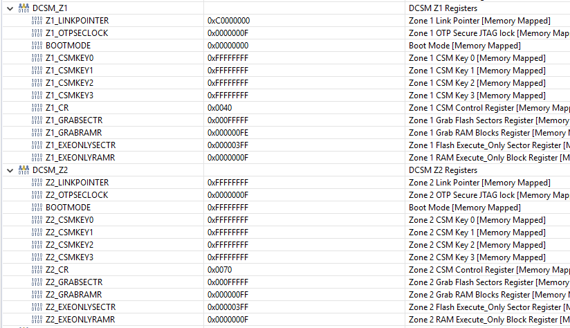
But the programming fails because of a Zone 1 Secure.

The GEL file used is : F28054F.gel

It's a new chip and, so far I know, non of of the secure settings are set.

If I read back the OTP Zone-1 reads all 0X0000 and Zone-2 reads all 0xFFFF

What's going wrong ?

  • Jan,

    You're correct that from the factory all zones should be unlocked/disabled.  I need to take a look at the GEL file when I get back to the office to confirm it is executing the correct unlock commands(even when the device is unlocked there is a procedure from RESET that has to be executed to unlock the device).

    In the meantime you can look at the registers described in http://www.ti.com/lit/spruhe5d starting at page 181 to see if there are things set that are not default.  I'd focus on the RAMSTAT register on this page, and then go to page 190 and look at Z1_CR to see if these bits indicate the dummy reads have not been done.

    I'll reply back tomm as soon as I look at the GEL to make sure it is correct.

    Best,

    Matthew

  • I have checked the mention registers and found:

    For the CR Registers

    So it seems the dummy reads are performed and some some password is stored for the Z1 zone.

    And for the RAMSTAT:

    So L0_RAM is secured

    Is this possible by a wrong setting of the JTAG or debug settings

    The security settings for the debugger for Zone1 and Zone 2 are :

    I hope you have an answer on short time because I can not go futher with he project and for each test we have to replace the processor.

    Thanks,
    jan

  • Hi Jan,

    Zone 1 definitely got programmed somehow. The Linkpointer has been programmed. The default should be 0xFFFFFFFF.

    Yes, it also appears RAM0 is locked to Zone 1 according to the RAMSTAT register.

    Unfortunately, because the Zone 1 link pointer has been programmed to 0xC0000000, you can not reprogram this and point to a new Zone Select Block.

    Therefore, it appears you will need a new part. And try to identify how this part got programmed to prevent it from happening again.

    sal

  • Thanks,

    that was also my conclusion, any suggestion to prevent writing to the OTP ?

    The linker map file shows that there are no sections of the OTP are used:

    Thanks,

    Jan

  • Hi Jan,

    Maybe you should carefully review the On chip Flash configuration in your CCS Debug session to make sure that you are not populating any of the OTP locations for programming. Start with a new target configuration file(.ccxml) and make sure the Security fields are all left to default. This will ensure that the “On Chip Flash” configuration in your ccxml is not the culprit. I am saying this because this is another way to program security settings to the device. This is my suggestion.

    Also check out this manual (section 6.3) which explains on how to debug the problems with Flash and what all precautions to follow while attempting a Flash Program/Erase operation. I suspect the Flash to be in depletion. Try Depletion recovery option in the On Chip Flash configuration. More details in the link below.

    http://www.ti.com/lit/an/spraal3/spraal3.pdf

    Thanks & Regards

    Pramod

  • Hi Jan,

    I think the device you are using is InstaSpin enabled hence on these devices TI secures  Zone1 (not programmed by your software). You need to use Zone2 only for security.

    Look like this info is missing in documentation. I'll raise a request to update the document to include this info. Sorry for the confusion and trouble you had with this issue.

    Regards,

    Vivek Singh

  • Thanks so I now know there is noting happen unexpected and go continue my project.

    But after startup it seem the motor parameters LS, Lq and Rs are not taken from the user.h file and are reading 0 or some random value.

    Has this something to do with the secured RAML0, if I use an other RAM location to initialize the estimator the right values are shown and everything woks fine.

    Regards,

    Jan

  • Yes, values in L0 should be all 0x0 (not sure what do you mean by random values). You should not use L0 for your application use.

    Regards,

    Vivek Singh

  • I am not using RAML0 for the application but initialize the estimator with the RAML0 location.

    And read the motor parameters with a EST function.

    The values for Rs, Lsd_H and LSq_H are zero or sometimes a unusual value f.i. Lsd_H = 1e30 H

    Regards,

    Jan

  • Jan,

    In earlier post you mentioned that if you use other RAM instead of RAML0 then it works fine. I would suggest to use other RAM in this case.

    Vivek Singh

  • Vivek,

    thanks for your reply that I can use on other location for the FAST RAM.

    But is there a reason for the fact I have to do this, because location 0x8000 is the default and advised setting in user.h.

    I like to understand what I am doing and why.

    Regards,

    Jan

  • Jan,

    Since it's secure RAM, it'll be difficult to understand the issue without running your code with proper setting. I'll request some one from motor control team to look into this and they have any suggestion.

    Regards,

    Vivek Singh

  • L0 RAM is reserved for InstaSPIN data, and should not be used by the customer. The instaSPIN libraries in ROM and L0 RAM are pre-allocated for the estimator are in the Z1 section. Make sure that the RAM utilized to place the variables used to interface with the instaSPIN library are accessible by the Z1 security zone.