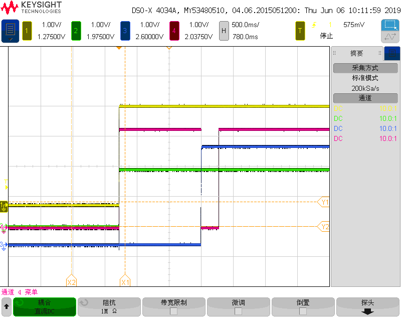
The 28335's power-up sequence must be 1.9V stable and then 3.3V open? Or can 3.3Vbe turned on after 1.9V reaches 0.7V? Is the power-on timing error causing the boot pin to be unstable?

-
Ask a related question
What is a related question?A related question is a question created from another question. When the related question is created, it will be automatically linked to the original question.