This thread has been locked.
If you have a related question, please click the "Ask a related question" button in the top right corner. The newly created question will be automatically linked to this question.
Tool/software: Code Composer Studio
I am trying to interface between TMS320F28377D and W5500 (WIZNET, Hardware TCP/IP IC).
I spent a lot of time for interfacing with them. But, I have in difficulty.
The below code is my code for SPIa module setting.
void Spia_init()
{
EALLOW;
DevCfgRegs.CPUSEL6.bit.SPI_A = 0; // select CPU1
CpuSysRegs.PCLKCR8.bit.SPI_A = 1; //select CPU Clock/
// GPIO_setting.
GpioCtrlRegs.GPBPUD.bit.GPIO54 = 0; // Enable pull-up on GPIO16 (SPISIMOA)
GpioCtrlRegs.GPBQSEL2.bit.GPIO54 = 3; // Asynch input GPIO16 (SPISIMOA)
GpioCtrlRegs.GPBGMUX2.bit.GPIO54=0;
GpioCtrlRegs.GPBMUX2.bit.GPIO54 = 1; // Configure GPIO16 as SPISIMOA
GpioCtrlRegs.GPBPUD.bit.GPIO55 = 0; // Enable pull-up on GPIO17 (SPISOMIA)
GpioCtrlRegs.GPBQSEL2.bit.GPIO55 = 3; // Asynch input GPIO17 (SPISOMIA)
GpioCtrlRegs.GPBGMUX2.bit.GPIO55=0;
GpioCtrlRegs.GPBMUX2.bit.GPIO55 = 1; // Configure GPIO17 as SPISOMIA
GpioCtrlRegs.GPBPUD.bit.GPIO56 = 0; // Enable pull-up on GPIO18 (SPICLKA)
GpioCtrlRegs.GPBQSEL2.bit.GPIO56 = 3; // Asynch input GPIO18 (SPICLKA)
GpioCtrlRegs.GPBGMUX2.bit.GPIO56=0;
GpioCtrlRegs.GPBMUX2.bit.GPIO56 = 1; // Configure GPIO18 as SPICLKA
GpioCtrlRegs.GPBPUD.bit.GPIO57 = 0; // Enable pull-up on GPIO57 (SPISTEA)
GpioCtrlRegs.GPBQSEL2.bit.GPIO57 = 3; // Asynch input GPIO57 (SPISTEA)
GpioCtrlRegs.GPBGMUX2.bit.GPIO57=0;
GpioCtrlRegs.GPBMUX2.bit.GPIO57 = 1; // Configure GPIO18 as SPICLKA
GpioCtrlRegs.GPAPUD.bit.GPIO23=0;
GpioCtrlRegs.GPAQSEL2.bit.GPIO23 = 3;
GpioCtrlRegs.GPAGMUX2.bit.GPIO23 = 0x0; // RST PIN for W5500
GpioCtrlRegs.GPAMUX2.bit.GPIO23 = 0x0;
EDIS;
SpiaRegs.SPICCR.bit.SPISWRESET = 0;
SpiaRegs.SPICCR.bit.CLKPOLARITY =1; // falling edge data transmission
SpiaRegs.SPICCR.bit.SPICHAR =7; //8-bit char
SpiaRegs.SPICTL.all = 0x0006; // Enable master mode, normal phase, Enable talk
SpiaRegs.SPIBRR.all = 0x001F; // Baud rate = LSPCLK/(BRR+1)
SpiaRegs.SPIFFTX.all = 0xE040; //Transmit registers
SpiaRegs.SPIFFRX.all = 0x2041; //Read registers
SpiaRegs.SPIFFCT.all = 0x00; // Transmit delay = no delay
SpiaRegs.SPIPRI.bit.FREE=1;
SpiaRegs.SPICCR.bit.SPISWRESET = 1;
}
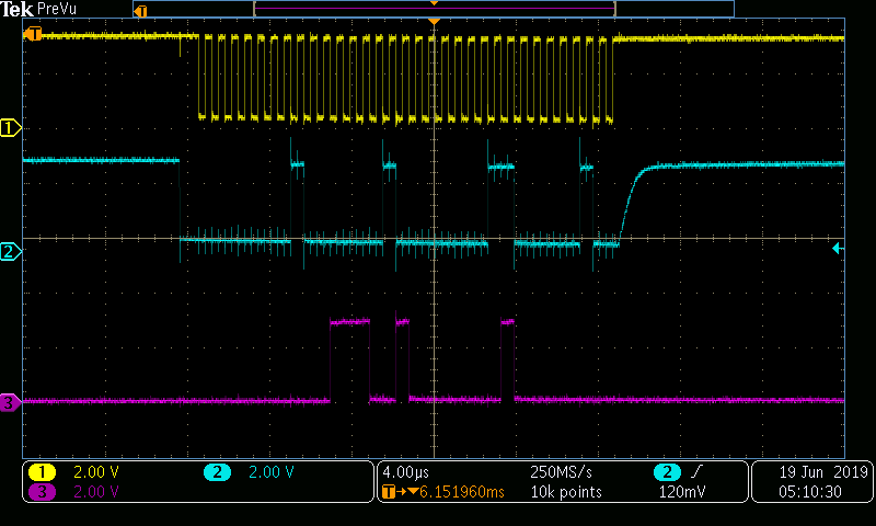
With aformentioned code, I have tried to confirm if the interface with W5500 is working well or not. Actually I expected what I would get wanted data If I send a certain command message (24bit) to W5500 as shown in below figure (from W5500 data sheet).
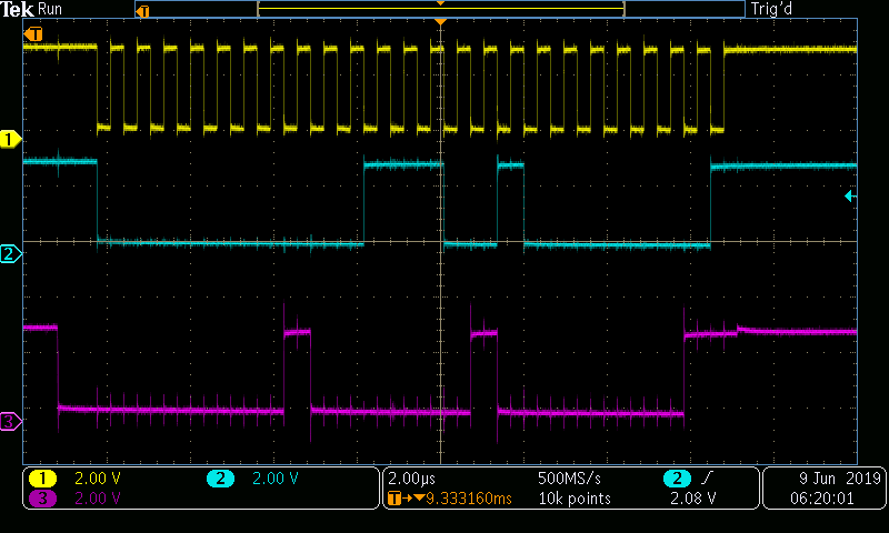
However, in my case, I failed to get data as shown in below figure (Ch. 1 (Yellow Line) : SPI_CLK, Ch.2 (Light Blue Line) : SPI_MOSI, Ch.3(Dark purple Line) : SPI_MISO
I don't understand a few situation related to the results
1) why the SPI_CLK and /SPITE signal finish before data is received from W5500.
2) What is the unwanted signal during Command transmission from TMS32028377D.
To solve the problem, could you give me review my SPIa setting code and any solution?
best regards
Sung-Ho Lee
Hi Sung-Ho Lee,
I see that you have used CLOCK_POLARITY=1 and CLOCK_PHASE=0 from your Master configurations. Can you confirm if the W5500 is also configured for the same configurations?
Also, can you please share the TX code(the code in which you are trying to transfer the command message)? It will help us to correlate the waveform you have shared.
Regards,
Praveen
Dear Praveen
Thank you for your kindly reply.
I confirmed W5500 configuration. its timing diagram as shown in enclosed file shows the data trasmission at falling edge and the data recieving at rising edge when SPI_CLK is high in idle.
And I send the functions related to data exchange using W5500
void WIZCHIP_WRITE(unsigned long AddrSel, unsigned int arg)
{
unsigned int i =0;
unsigned int Send_Cmd[3] = {0,};
AddrSel |= (_W5500_SPI_WRITE_ | _W5500_SPI_VDM_OP_);
Send_Cmd[0]= (AddrSel&0x00FF0000)>>16;
Send_Cmd[1]= (AddrSel&0x0000FF00)>>8;
Send_Cmd[2]= (AddrSel&0x000000FF);
//CS_ON// Use SPISTEA manually
for(i=0; i<3; i++)
{
SpiaRegs.SPITXBUF=(Send_Cmd[i]<<8); // Send cmd
}
SpiaRegs.SPITXBUF=arg<<8; // Send data
while(!SpiaRegs.SPIFFTX.bit.TXFFST){}
//CS_OFF// Use SPISTEA manually
}
unsigned int WIZCHIP_READ(unsigned long AddrSel) //unsigned int COMMON_REG_READ_byte(unsigned int Addr_off);
{
unsigned int rcv_data;
unsigned int i=0;
unsigned int Send_Cmd[3]={0,};
if(!SpiaRegs.SPIFFRX.bit.RXFFST) SpiaRegs.SPIFFRX.bit.RXFIFORESET =0; SpiaRegs.SPIFFRX.bit.RXFIFORESET =1;
AddrSel |= (_W5500_SPI_READ_ | 1);
Send_Cmd[0]= (AddrSel&0x00FF0000)>>16;
Send_Cmd[1]= (AddrSel&0x0000FF00)>>8;
Send_Cmd[2]= (AddrSel&0x000000FF);
//CS_ON// Use SPISTEA manually
for(i=0; i<3; i++)
{
SpiaRegs.SPITXBUF=(Send_Cmd[i]<<8); // Send cmd
}
rcv_data=(SpiaRegs.SPIRXBUF>>8); // recieve data
//while(!SpiaRegs.SPIFFRX.bit.RXFFST){;;}
//CS_OFF// Use SPISTEA manually
return rcv_data;
}
In main(), I only call the functions.
Best regards
Sung-Ho Lee
Hi Sung-Ho Lee,
Thanks for the confirmation.
According to the SPI protocol, the Master node generates the CLK whenever there is data written in the TXBUF. According to the code you have shared, I see there are only 3 x 8Bit data written in the WIZCHIP_READ function, hence you see 24 clocks and the corresponding data on SIMO.
If you require CLK to be generated for receiving data packets beyond 24bits of Command packets, I suggest you should initiate a dummy Master transmit of say 8 bits(if you are expecting a 8 bit data from the slave node) after transferring the Command packets.
Can you try with dummy TXBUF writes?
Regards,
Praveen
Hi Sung-Ho Lee,
Were you able to try out the suggestions? Any luck?
Regards,
Praveen
Dear Praveen
I am sorry for late response..
I tried to test according to your suggestions
Please see the below code that added dummy.
unsigned int WIZCHIP_READ(unsigned long AddrSel) //unsigned int COMMON_REG_READ_byte(unsigned int Addr_off);
{
unsigned int rcv_data;
unsigned int i=0;
unsigned int Send_Cmd[4]={0,};
if(!SpiaRegs.SPIFFRX.bit.RXFFST) SpiaRegs.SPIFFRX.bit.RXFIFORESET =0; SpiaRegs.SPIFFRX.bit.RXFIFORESET =1;
AddrSel |= (_W5500_SPI_READ_ | 1);
Send_Cmd[0]= (AddrSel&0x00FF0000)>>16;
Send_Cmd[1]= (AddrSel&0x0000FF00)>>8;
Send_Cmd[2]= (AddrSel&0x000000FF);
Send_Cmd[3]=0; //Dummy
//CS_ON// Use SPISTEA manually
for(i=0; i<4; i++)
{
SpiaRegs.SPITXBUF=(Send_Cmd[i]<<8); // Send cmd
}
rcv_data=(SpiaRegs.SPIRXBUF>>8);
//while(!SpiaRegs.SPIFFRX.bit.RXFFST){;;}
//CS_OFF// Use SPISTEA manually
return rcv_data;
}
Although the addition of dummy data after sending Command packets, it shows the same results as shown in below figure
(Ch. 1 <Yellow line>: SPI CLK, Ch. 2<light blue line>: MISO, Ch. 3<Deep purple line>: MOSI )
As you can see, before finishing sending command packet (24bit), the unwanted data is imported.
In addition, I found both RX(MISO) and TX(MOSI) signals transimit or receive the data on the negative edge of the SPI CLK singal.
My SPI Setting code is as follows:
void Spia_init(void)
{
EALLOW;
DevCfgRegs.CPUSEL6.bit.SPI_A = 0; // select CPU1
CpuSysRegs.PCLKCR8.bit.SPI_A = 1; //select CPU Clock/
// GPIO_setting.
GpioCtrlRegs.GPBPUD.bit.GPIO54 = 0; // Enable pull-up on GPIO54 (SPISIMOA)
GpioCtrlRegs.GPBQSEL2.bit.GPIO54 = 3; // Asynch input GPIO54 (SPISIMOA)
GpioCtrlRegs.GPBGMUX2.bit.GPIO54=0;
GpioCtrlRegs.GPBMUX2.bit.GPIO54 = 1; // Configure GPIO54 as SPISIMOA
GpioCtrlRegs.GPBPUD.bit.GPIO55 = 0; // Enable pull-up on GPIO55 (SPISOMIA)
GpioCtrlRegs.GPBQSEL2.bit.GPIO55 = 3; // Asynch input GPIO55 (SPISOMIA)
GpioCtrlRegs.GPBGMUX2.bit.GPIO55=0;
GpioCtrlRegs.GPBMUX2.bit.GPIO55 = 1; // Configure GPIO56 as SPISOMIA
GpioCtrlRegs.GPBPUD.bit.GPIO56 = 0; // Enable pull-up on GPIO56 (SPICLKA)
GpioCtrlRegs.GPBQSEL2.bit.GPIO56 = 3; // Asynch input GPIO56 (SPICLKA)
GpioCtrlRegs.GPBGMUX2.bit.GPIO56=0;
GpioCtrlRegs.GPBMUX2.bit.GPIO56 = 1; // Configure GPIO56 as SPICLKA
GpioCtrlRegs.GPBPUD.bit.GPIO57 = 0; // Enable pull-up on GPIO57 (SPISTEA)
GpioCtrlRegs.GPBQSEL2.bit.GPIO57 = 3; // Asynch input GPIO57 (SPISTEA)
GpioCtrlRegs.GPBGMUX2.bit.GPIO57=0;
GpioCtrlRegs.GPBMUX2.bit.GPIO57 = 1; // Configure GPIO57 as SPICLKA
GpioCtrlRegs.GPAPUD.bit.GPIO23=0;
GpioCtrlRegs.GPAQSEL2.bit.GPIO23 = 3;
GpioCtrlRegs.GPAGMUX2.bit.GPIO23 = 0; // RST PIN for W5500
GpioCtrlRegs.GPAMUX2.bit.GPIO23 = 0;
EDIS;
SpiaRegs.SPICCR.bit.SPISWRESET = 0;
SpiaRegs.SPICCR.bit.CLKPOLARITY =1; // falling edge data transmission
SpiaRegs.SPICCR.bit.SPICHAR =7; //8-bit char
SpiaRegs.SPICTL.all = 0x0006; // Enable master mode, normal phase, Enable talk
SpiaRegs.SPIBRR.all = 0x001F; // Baud rate = LSPCLK/(BRR+1)
SpiaRegs.SPIFFTX.all = 0xE040; //Transmit registers
SpiaRegs.SPIFFRX.all = 0x2041; //Read registers
SpiaRegs.SPIFFCT.all = 0x00; // Transmit delay = no delay
SpiaRegs.SPIPRI.bit.FREE=1;
SpiaRegs.SPICCR.bit.SPISWRESET = 1;
}
I have not yet found what the cause of the problem is.
best regards
Sung-Ho Lee
Hi Sung-Ho Lee,
The unwanted data seems to be coming from the SPI slave(W5500 in your case). You may have to check this from the W5500 spec on why this is happening. I would suggest to start looking for the below from the W5500 spec:
Regarding the comment below:
"In addition, I found both RX(MISO) and TX(MOSI) signals transimit or receive the data on the negative edge of the SPI CLK singal."
This is in accordance with the SPI mode that is configured. The data is launched at negative edge and will be sampled on positive edge.Please refer to the datasheet Figure 5-68 for reference.
Regards,
Praveen
Hi Sung-Ho Lee,
I haven’t heard from you for 2 weeks, so I’m assuming you were able to resolve your issue. If this isn’t the case, please click the "This did NOT resolve my issue" button and reply to this thread with more information. If this thread locks, please click the "Ask a related question" button and in the new thread describe the current status of your issue and any additional details you may have to assist us in helping to solve your issues.
Regards,
Praveen