This thread has been locked.

If you have a related question, please click the "Ask a related question" button in the top right corner. The newly created question will be automatically linked to this question.

CCS/TMS320F28335: ADC Hardware Design - Against EMI

Part Number: TMS320F28335

Tool/software: Code Composer Studio

Hi, 

I am using DSP in my power electronics converter project.

In my application, DSP needs to read boost converter output voltage with ADC(to provide feedback). 

However, a larger EMI comes from a high frequency large current resonant converter close to the DSP. So the ADC result is not stable, even after calculating average from every 20 samples. 

Here is my circuit sampling boost output voltage and feed to ADC. 

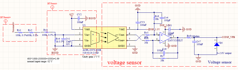
I plan to add a ferrite bead in series with Rv9 to help filter EMI. 

Question:

1. Is there any problem with my circuit design?

2. What else can I do to filter EMI? 

Any suggestion will help!

Thank you!

Xiaoming Wang

  • Xiaoming,

    I've assigned your post to a C2000 expert, but due to the US holiday we will get back to you no later than July 8th, by end of day US Central Time.

    Best regards,
    Matthew

  • Hi Matthew,

    Didn't hear from you these days. Do you get any feedback?

    Thank you !

    Xiaoming

  • Xiaoming,

    I apologize for the lateness from our side.  Here are some thoughts I have:

    1)Is it possible to convert the ADC input with resonant converter idle, to verify what component of the code spread is coming from the EMI?  I want to make sure the behaivor of the ideal state is normal

    2)Typically op-amps behave non-ideally with large capacitive loads, and to counter-act this a series resistor is recommended to help stabilize the output.  I see you have done this with a 100ohm resistor.  Looking at the resistances on the inputs, which are 20k, we might try a resistor of the same order on the output for matching reasons.  

    3)Location of passives: for the final decoupling cap at the ADC input placing this component as close as possible to the physical pin will be best in terms of EMI immunity.  Not sure of your layout locations, etc.  Given this ADC design I would also place the same importance on the 2.2uF caps on ADCREFP/REFM pins as well as the RESEXT resistor.  The connection of the ADCLO pin needs to be as short/direct to the ground plane as well.

    I've asked some of the folks in our digital power team to take a look at this as well to see if they have any unique concerns when implementing a resonant converter topology vs EMI.

    Best,

    Matthew

  • Hi Matthew,

    Thank you for your quick response!

    I will try your first suggestion to determine the source of noise. 

    For the second point, I look through an application report SPRAAP6A. On page 6, I see a suggestion that the input resistance should <50ohm. What do you think?

    For the third suggestion, let me show you my DSP sch ADC part. 

    Capacitors and resistors are as close as possible to the corresponding pins. Is the design good?

    Regards,

    Xiaoming 

  • Hi Matthew, 

    I don't have electronic load to run boost converter but I was able to remove a EMI source(a big inductor) from resonant board. I do see the output of boost gets stabler than before, though it is still shaking. 

    For my last reply, figure 1 should be the following screenshot.

    Sorry for the inconvenience. 

    Looking forward to your reply.

    Regards, 

    Xiaoming

  • Xiaoming,

    Your post with the passives on the ADC is good in terms of meeting the DS requirement, but I would also look at the layout and make sure the passives as as close to the device as possible.  Any extra wire trace between the passive and the pin will gradually couple in more noise from the system.

    For the op-amp, the last paragraph is referring to the inside of the chip/design, there isn't anything you can do about that circuit other than know the values(which we provide in the DS).

    For the external passives on the output of the op-amp, these would need to satisfy the RC equation for charging the S/H cap inside the device as well as meet any specs the op-amp has for stability.

    Best,

    Matthew

  • Hi Matthew,

    Thank you for your reply!

    Here are schematic and PCB design of ADC part of DSP28335. 

    DSP and boost converter are on separate boards so I use jumper wires for signal connection. Opamp is on boost board. I am afraid the jumper wires are absorbing EMI. 

    One more question on the code side, how does ACQ_PS register in ADCTRL affect the accuracy of ADC? 

    Thank you!

    Regards,

    Xiaoming

  • The jumpers could be acting as an antennae, certainly the shorter the better; and if you can run a ground wire in the bundle it may help.

    ACQ_PS register controls the amount of time the S/H cap inside the MCU is allowed to sample the external signal.  So, for example, if you had a larger resistive load on the ADC input, you could use an larger ACQ_PS value to allow the internal S/H cap more time to charge/settle.  

    You could try larger values to see if it might help average out the EMI you are seeing as well; additionally you could move your sample trigger to see if the EMI event could be avoided altogether.

    Best,

    Matthew