This thread has been locked.

If you have a related question, please click the "Ask a related question" button in the top right corner. The newly created question will be automatically linked to this question.

TMS320F280049: unexpected behavior when F280049 fail to run

Part Number: TMS320F280049
Other Parts Discussed in Thread: LM1117

Hi Team,


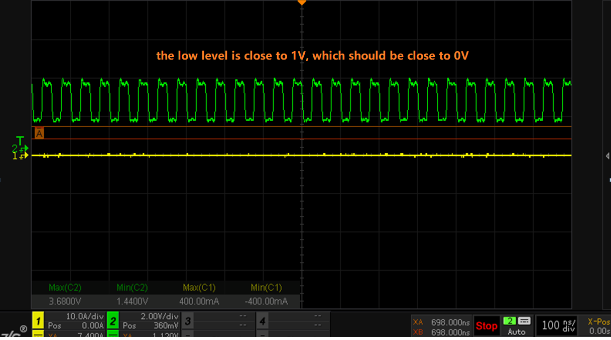
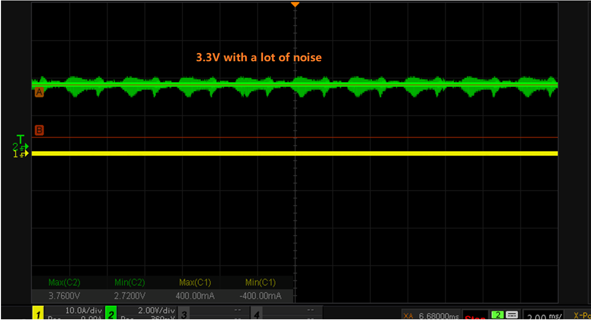
My customer are using F280049 for three phase OBC control, five pwms output is low, but one pwm is continual high, there will have occasionally that F280049 fail to run, the external oscillator waveform is abnormal, 3.3V and 1.2V output have a lot of noise as below:


After warm reset F28004x by hand, the external oscillator waveform, 3.3V and 1.2V output are normal


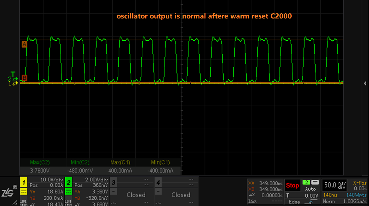
After warm reset F28004x by hand, the external oscillator waveform, 3.3V and 1.2V output are normal.

We guess this issue was cause by missing clock, Customer configure TZ5 to shut down all pwm when clock fail, and also configure NMI interrupt to shut down pwms. Also they configure watchdog, but apparently the watchdog did not work. there are two things that hard to explain:

1. Why there still have one pwm output high when configure TZ5 to shut down all pwm? This function have been verify in the lab by disconnecting external clock and all pwms output are low.

2. What cause the external oscillator waveform abnormal, and 3.3V and 1.2V output have a lot of noise? The 3.3V is provide by LM1117,  As it is not easy to reproduce this issue, in normal running condition, customer did the test that by adding additional 500mA resistor load for LM1117, the 3.3V and 1.2V output is normal without noise.

Customer used to try F280049 internal clock, but still have possibility that F280049 fail to run. We help review customer schematic, there is no over voltage design on ADC and GPIO pins, and the VDDA, VDD, VDDIO, Reset pin are connected according to datasheet recommendation. Any suggestion for customer to avoid this issue?

  • Strong,

    Due to US holiday we will reply back no later than July 8th by end of day US central time.

    Best,

    Matthew

  • Strong,

    It is hard to tell what is going on here, the large magnitude noise on the supply suggests some system level contention.

    A few preliminary questions.

    - Is the input clock a crystal between X1/X2 or is it a single ended 3.3v input to X1 from an oscillator?

    - Is there a 1.2v external LDO or are they using the F28049 internal LDO VREG or DCDC?

    Best regards,

    Jason

  • Hi Jason,

    here are the input:

     -Is the input clock a crystal between X1/X2 or is it a single ended 3.3v input to X1 from an oscillator?

    ---- actually they have try both of the external clock, use single ended 3.3v input to X1 from an oscillator can reduce the possibility of fail, but still can not avoid.

    - Is there a 1.2v external LDO or are they using the F28049 internal LDO VREG or DCDC?

    ----  they are using the F28049 internal LDO VREG when they try internal clock.

  • Hi Strong,

    Did customer look at their board schematic to see if their was any issue with ground reference? Does this issue still persist? If not please, close this thread.

    Thanks,

    Nirav

  • Hi Nirav,

    I have help review customer's schematic and did not find issue, Customer can not send the schematic for your review, this issue still persist.

    Strong

  • Hi Strong,

    We need more information from customer side in order to debug, since this issue appears to be board related.

    I will go ahead and close this thread for now. If you get more details from customer please go ahead and re-open this thread or start a new one.

    Thanks & Regards,

    Nirav