Part Number: TMS320F28021
Hi Team,
I have some questions about the behavior of Ch capacitor during for example SOC0 to SOC1 conversion process.
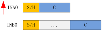
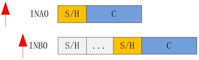
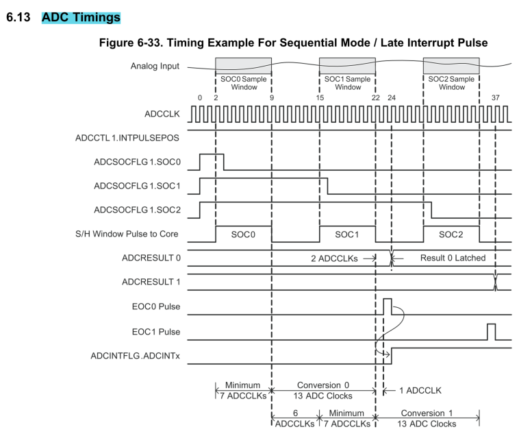
1. The switch is closed during S/H window, and the Ch will be charged by Cp and Cs capacitors. My question is that what's the behavior from the end of S0C0 S/H window to the beginning of SOC1 S/H window. Will Ch discharges completely, why or why not? How to make sure the next sampling is correct?
2. Is F2802x ADC sampling process same with F28004x and F2837xd(12-bit mode), and could we refer their computational formulas for F2802x to calculate the S+H duration?
Thanks!

-Rayna