This thread has been locked.

If you have a related question, please click the "Ask a related question" button in the top right corner. The newly created question will be automatically linked to this question.

TMS320F280049: ADC pin to GND impedance during power down


Hi team,

My customer is designing a system with high requirement of stand-by power consumption. 

To achieve lowest power consumption, they power off the c2000 power rail. When input voltage recovers, they re-enable the power rail to power up C2000.

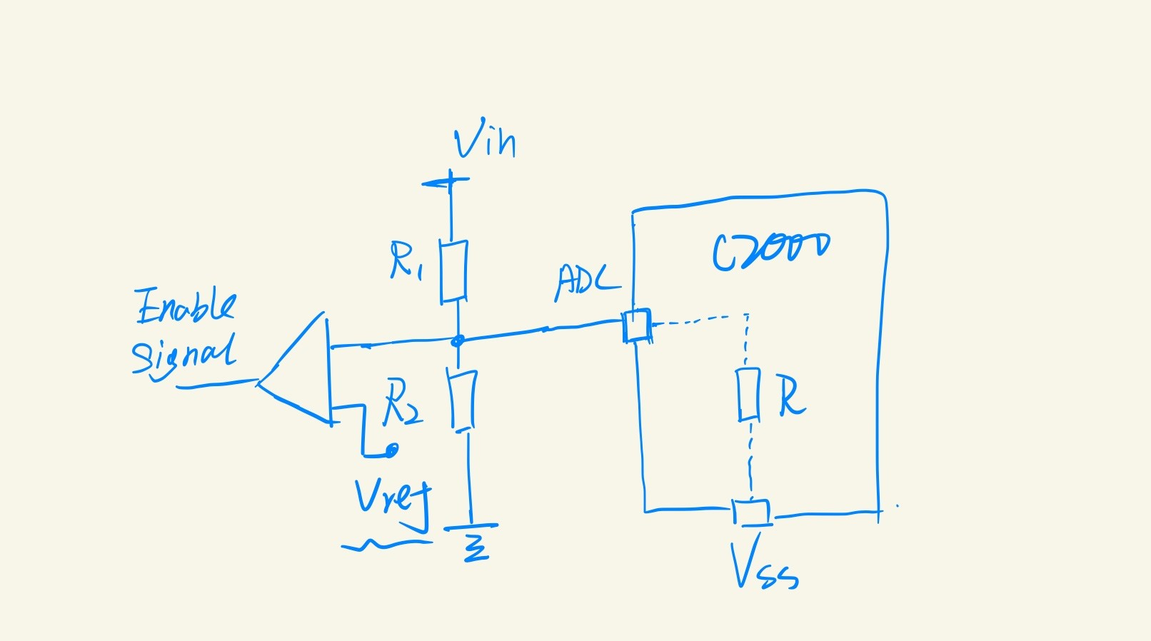
In this system, input voltage is sample by series shunt resistors R1 and R2. When C2000 power off, the voltage on R2 is compared with a Vref. When Vin rise up, a output voltage level will be generated by comparator to enable the power rail of C2000.

The problem is when C2000 is powered off the internal impedance R becomes small (10k according to their measurement). Thus the voltage on R2 will be influenced by R since R and R2 is in parallel. And Vref should also be adjusted accordingly.

Thus, customer wants to know the range of internal 'R' when C2000 is powered-off to calculate the correct value of Vref.

Hope I've made everything clear.

Regards,

Brian

  • Hi Brian,

    If the ADC input is about 0.3V above VDDA, the ESD diodes will turn on.  The current will not be linear with voltage (can't be modeled with an 'R') and will be highly temperature dependent.  

    I'd recommend buffering the sensed voltage with an op-amp with an enable.  This will allow the voltage to be isolated when the MCU is powered down and you should also be able to increase the R values of the voltage divider, resulting in lower static power dissipation.  

  • Brian,

    Have they considered using XRSn > ~2.8V as the ENABLE signal?

    -Tommy

  • Hi Tommy,

    I am sorry that did not get your idea.

    As I mentioned above, when system goes into low power mode, the power rail for VDD will be disabled. In this way, I am afraid they cannot get a >2.8V XRSn.

    Or maybe it is a totally different idea? More ideas are welcomed

    They reason why they would like to power down 280049 is they cannot reduce the power consumption below 1mA, which made it very hard for them to meet the system power consumption requirement.

    Regards,

    Brian

  • Hi Devin,

    Since this is a highly cost sensitive project, customer would not consider adding another buffer.

    In fact, regarding that the sensed voltage would only be 0 or rated, they do not need to know a very accurate internal resistance. Only need a range to guarantee they could set proper Vref for the comparator.

    Regards,

    Brian 

  • Brian,

    The drawing is confusing to me.  What is the ENABLE signal controlling?  I was under the impression that the C2000 was the controller on the board that would power up first and then send an ENABLE signal to the rest of the system to power on.  Are they implementing the reverse?  Is the ENABLE signal used to release power to the C2000?

    What is the purpose for the C2000 ADC connected to the voltage divider?  Is it required for monitoring the Vin supply at run-time?

    -Tommy

  • Hi Brian,

    We can't give a resistance estimate because this is not a resistor and shouldn't be modeled as such.  

    Probably they need to simulate in SPICE with a variety of silicon diodes at a variety of temperatures to see if there is a viable threshold that can be set to accurately discriminate between good and too-low voltages.  Adding some series resistance to the ADC input will limit the clamping current which will help the voltage divider remain more stable.  Of course this will slow down ADC input settling in the actual application.  

    Characterizing the behavior of multiple copies of the actual system over a variety of conditions could also be viable. 

    In all cases, it is imperative that the clamping current not violate the clamping current specification in the absolute max ratings table in the datasheet, otherwise the device could be permanently damaged.  As-is, if they see about 0.3mA of current, that should be OK as the clamping specification is 20mA (although note that this is a sum of all inputs on the device, not per-input) plus they will want low clamping current since they want low overall current.    

  • Since the power consumption is too high for their overall stand-by requirement.

    Thus, they decide to cut off C2000 in stand-by state by disable the power rail of C2000. And they use another signal to enable C2000 power rail when the system goes back to normal state. 

    Yes, the enable signal is used to release power fo C2000 and it happens to connected with C2000. 

  • Hi Devin,

    I understand your concern.

    However, from the customer point of view, they have no visibility to the internal of our chip. Thus, they need TI's instruction on this topic to make sure their design is robust. So we cannot just recommend customer to confirm the voltage threshold by testing.

    I think the TINA simulation is a good idea. Could you help to provide a model of C2000 to help customer understand what is going on inside C2000? 

    Regards,

    Brian 

  • Brian,

    I do not think the proposed topology will work.

    As Devin mentioned, there is a diode from the ADC inputs to VDDA.  This will turn on in this condition and the op-amp supply detection circuit will not work.

    A blocking/isolation circuit such as another opamp or pass gate between the op-amp and the F280049 will be needed.  Perhaps replicating a duplicate R1 and R2 for the supply detection circuit separate from the ADC input could work as well, but the customer should still take care not to apply a voltage to the ADC input before the VDDA is powered with an isolation circuit enabled by the same enable.

    Best regards,

    Jason 

  • Hi Jason,

    Thanks for the comments.

    And I agree with you and Devin that we need an extra circuit to isolate the enable signal.

    I have suggested customer to add a buffer. When C2000 power down, the amplifier will power down together. And the signal on the input end of amplifier is used as the enable signal to power up the C2000 and amplifier together. By doing this, they can isolate the enable signal to avoid potential problem and will not influence the sampling.

    Thanks!

    Brian