


Part Number: TMS320F280049
Other Parts Discussed in Thread: C2000WARE
I have a question about EPWM for F280049.
This PWM setting is based on the following sample program “Active high complementary PWMs” provided by TI.
...\ti\c2000\C2000Ware_2_00_00_02\device_support\f2805x\examples\c28\epwm_deadband\Example_2805xEPwmDeadBand.c
void InitEPwm3Example()
When TBCTR = 0, this PWM setting has been changed so that EPWMxA output becomes HIGH.
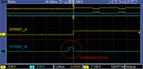
An unexpected pulse is generated at startup as shown below.
Please tell me the cause and countermeasure.
The programs that cause this problem are listed below.
The change code is shown in red.
**********************************************************************************************************************
//
// Defines
//
//
// Maximum Dead Band values
//
#define EPWM1_MAX_DB   0x03FF
#define EPWM2_MAX_DB   0x03FF
#define EPWM3_MAX_DB   0x03FF

#define EPWM1_MIN_DB   0
#define EPWM2_MIN_DB   0
#define EPWM3_MIN_DB   0

//
// TBCTL (Time-Base Control)
//

//
// CTRMODE bits
//
#define TB_COUNT_UP      0x0
#define TB_COUNT_DOWN    0x1
#define TB_COUNT_UPDOWN  0x2
#define TB_FREEZE        0x3

//
// PHSEN bit
//
#define TB_DISABLE  0x0
#define TB_ENABLE   0x1

//
// PRDLD bit
//
#define TB_SHADOW     0x0
#define TB_IMMEDIATE  0x1

//
// SYNCOSEL bits
//
#define TB_SYNC_IN       0x0
#define TB_CTR_ZERO      0x1
#define TB_CTR_CMPB      0x2
#define TB_SYNC_DISABLE  0x3

//
// HSPCLKDIV and CLKDIV bits
//
#define TB_DIV1   0x0
#define TB_DIV2   0x1
#define TB_DIV4   0x2

//
// PHSDIR bit
//
#define TB_DOWN   0x0
#define TB_UP     0x1

//
// CMPCTL (Compare Control)
//

//
// LOADAMODE and LOADBMODE bits
//
#define CC_CTR_ZERO      0x0
#define CC_CTR_PRD       0x1
#define CC_CTR_ZERO_PRD  0x2
#define CC_LD_DISABLE    0x3

//
// SHDWAMODE and SHDWBMODE bits
//
#define CC_SHADOW     0x0
#define CC_IMMEDIATE  0x1

//
// AQCTLA and AQCTLB (Action Qualifier Control)
//

//
// ZRO, PRD, CAU, CAD, CBU, CBD bits
//
#define AQ_NO_ACTION  0x0
#define AQ_CLEAR      0x1
#define AQ_SET        0x2
#define AQ_TOGGLE     0x3

//
// DBCTL (Dead-Band Control)
//

//
// OUT MODE bits
//
#define DB_DISABLE      0x0
#define DBB_ENABLE      0x1
#define DBA_ENABLE      0x2
#define DB_FULL_ENABLE  0x3

//
// POLSEL bits
//
#define DB_ACTV_HI   0x0
#define DB_ACTV_LOC  0x1
#define DB_ACTV_HIC  0x2
#define DB_ACTV_LO   0x3

//
// IN MODE
//
#define DBA_ALL          0x0
#define DBB_RED_DBA_FED  0x1
#define DBA_RED_DBB_FED  0x2
#define DBB_ALL          0x3

//
// CHPCTL (chopper control)
//

//
// CHPEN bit
//
#define CHP_DISABLE  0x0
#define CHP_ENABLE   0x1

//
// CHPFREQ bits
//
#define CHP_DIV1  0x0
#define CHP_DIV2  0x1
#define CHP_DIV3  0x2
#define CHP_DIV4  0x3
#define CHP_DIV5  0x4
#define CHP_DIV6  0x5
#define CHP_DIV7  0x6
#define CHP_DIV8  0x7

//
// CHPDUTY bits
//
#define CHP1_8TH  0x0
#define CHP2_8TH  0x1
#define CHP3_8TH  0x2
#define CHP4_8TH  0x3
#define CHP5_8TH  0x4
#define CHP6_8TH  0x5
#define CHP7_8TH  0x6

//
// TZSEL (Trip Zone Select)
//

//
// CBCn and OSHTn bits
//
#define TZ_DISABLE  0x0
#define TZ_ENABLE   0x1

//
// TZCTL (Trip Zone Control)
//

//
// TZA and TZB bits
//
#define TZ_HIZ       0x0
#define TZ_FORCE_HI  0x1
#define TZ_FORCE_LO  0x2
#define TZ_NO_CHANGE 0x3

//
// TZDCSEL (Trip Zone Digital Compare)
//

//
// DCAEVT1, DCAEVT2, DCBEVT1, DCBEVT2 bits
//
#define TZ_EVT_DISABLE      0x0
#define TZ_DCAH_LOW         0x1
#define TZ_DCAH_HI          0x2
#define TZ_DCAL_LOW         0x3
#define TZ_DCAL_HI          0x4
#define TZ_DCAL_HI_DCAH_LOW 0x5

#define TZ_DCBH_LOW         0x1
#define TZ_DCBH_HI          0x2
#define TZ_DCBL_LOW         0x3
#define TZ_DCBL_HI          0x4
#define TZ_DCBL_HI_DCBH_LOW 0x5

//
// ETSEL (Event Trigger Select)
//
#define ET_DCAEVT1SOC   0x0
#define ET_CTR_ZERO     0x1
#define ET_CTR_PRD      0x2
#define ET_CTR_PRDZERO  0x3
#define ET_CTRU_CMPA    0x4
#define ET_CTRD_CMPA    0x5
#define ET_CTRU_CMPB    0x6
#define ET_CTRD_CMPB    0x7

//
// ETPS (Event Trigger Pre-scale)
//

//
// INTPRD, SOCAPRD, SOCBPRD bits
//
#define ET_DISABLE  0x0
#define ET_1ST      0x1
#define ET_2ND      0x2
#define ET_3RD      0x3

 //
    // Step 4. Initialize all the Device Peripherals:
    // Not required for this example
    EALLOW;
    CpuSysRegs.PCLKCR0.bit.TBCLKSYNC = 0;

    // GPIO Configuration
    GpioCtrlRegs.GPAMUX1.bit.GPIO4 = 1;   // Configure GPIO4 as EPWM3A
    GpioCtrlRegs.GPAMUX1.bit.GPIO5 = 1;   // Configure GPIO5 as EPWM3B
    EDIS;

    EPwm3Regs.TBPRD = 6000;                         // Set timer period
    EPwm3Regs.TBPHS.bit.TBPHS = 0x0000;            // Phase is 0
    EPwm3Regs.TBCTR = 0x0000;                       // Clear counter

    //
    // Setup TBCLK
    //
    EPwm3Regs.TBCTL.bit.CTRMODE = TB_COUNT_UPDOWN; // Count up
    EPwm3Regs.TBCTL.bit.PHSEN = TB_DISABLE;        // Disable phase loading
    EPwm3Regs.TBCTL.bit.HSPCLKDIV = TB_DIV4;       // Clock ratio to SYSCLKOUT
    EPwm3Regs.TBCTL.bit.CLKDIV = TB_DIV4;          // Slow to observe on scope

    //
    // Setup compare
    //
    EPwm3Regs.CMPA.bit.CMPA = 3000;

    //
    // Set actions
    //
    EPwm3Regs.AQCTLA.bit.ZRO = AQ_SET;              // Set PWM3A on Zero
    EPwm3Regs.AQCTLA.bit.CAD = AQ_CLEAR;


    EPwm3Regs.AQCTLB.bit.CAU = AQ_CLEAR;            // Set PWM3A on Zero
    EPwm3Regs.AQCTLB.bit.CAD = AQ_SET;

    //
    // Active high complementary PWMs - Setup the deadband
    //
    EPwm3Regs.DBCTL.bit.OUT_MODE = DB_FULL_ENABLE;
    EPwm3Regs.DBCTL.bit.POLSEL = DB_ACTV_HIC;
    EPwm3Regs.DBCTL.bit.IN_MODE = DBA_ALL;
    EPwm3Regs.DBRED.all = EPWM3_MIN_DB;
    EPwm3Regs.DBFED.all = EPWM3_MIN_DB;

    //
    // Interrupt where we will change the deadband
    //
    EPwm3Regs.ETSEL.bit.INTSEL = ET_CTR_ZERO;     // Select INT on Zero event
    EPwm3Regs.ETSEL.bit.INTEN = 1;                // Enable INT
    EPwm3Regs.ETPS.bit.INTPRD = ET_3RD;           // Generate INT on 3rd event

    EALLOW;
    CpuSysRegs.PCLKCR0.bit.TBCLKSYNC = 1;
    EDIS;
**********************************************************************************************************************
