Hi expert,
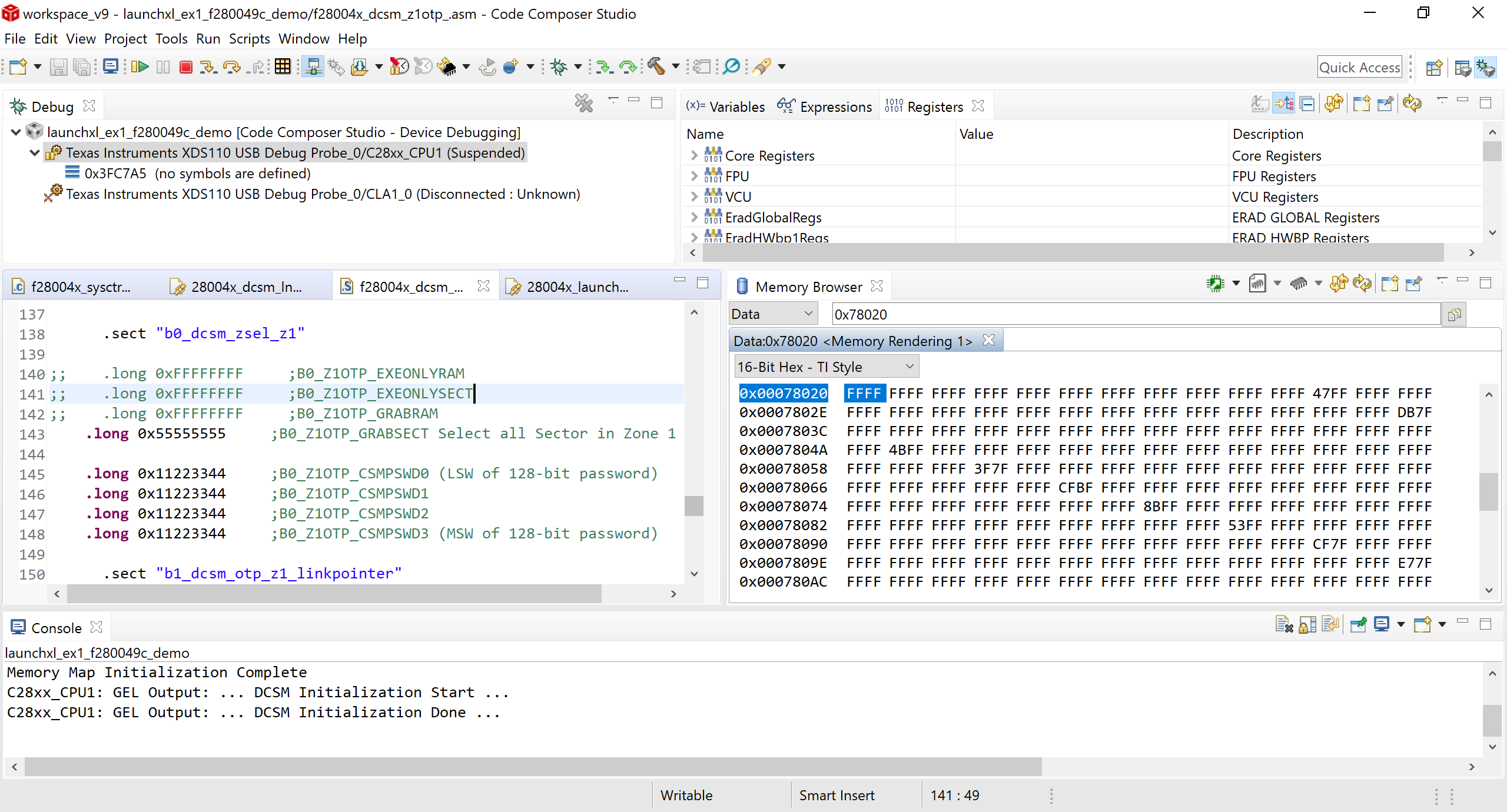
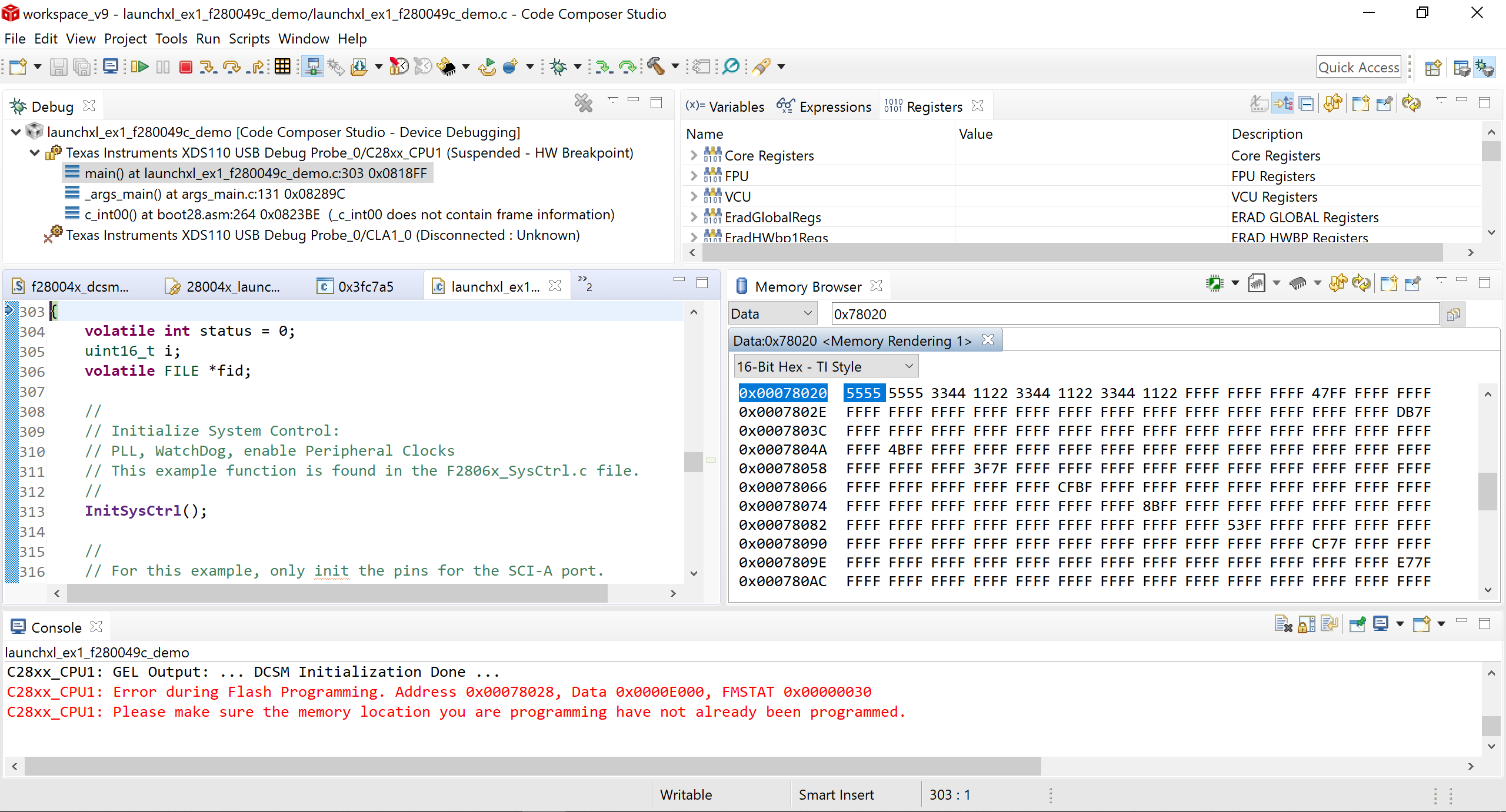
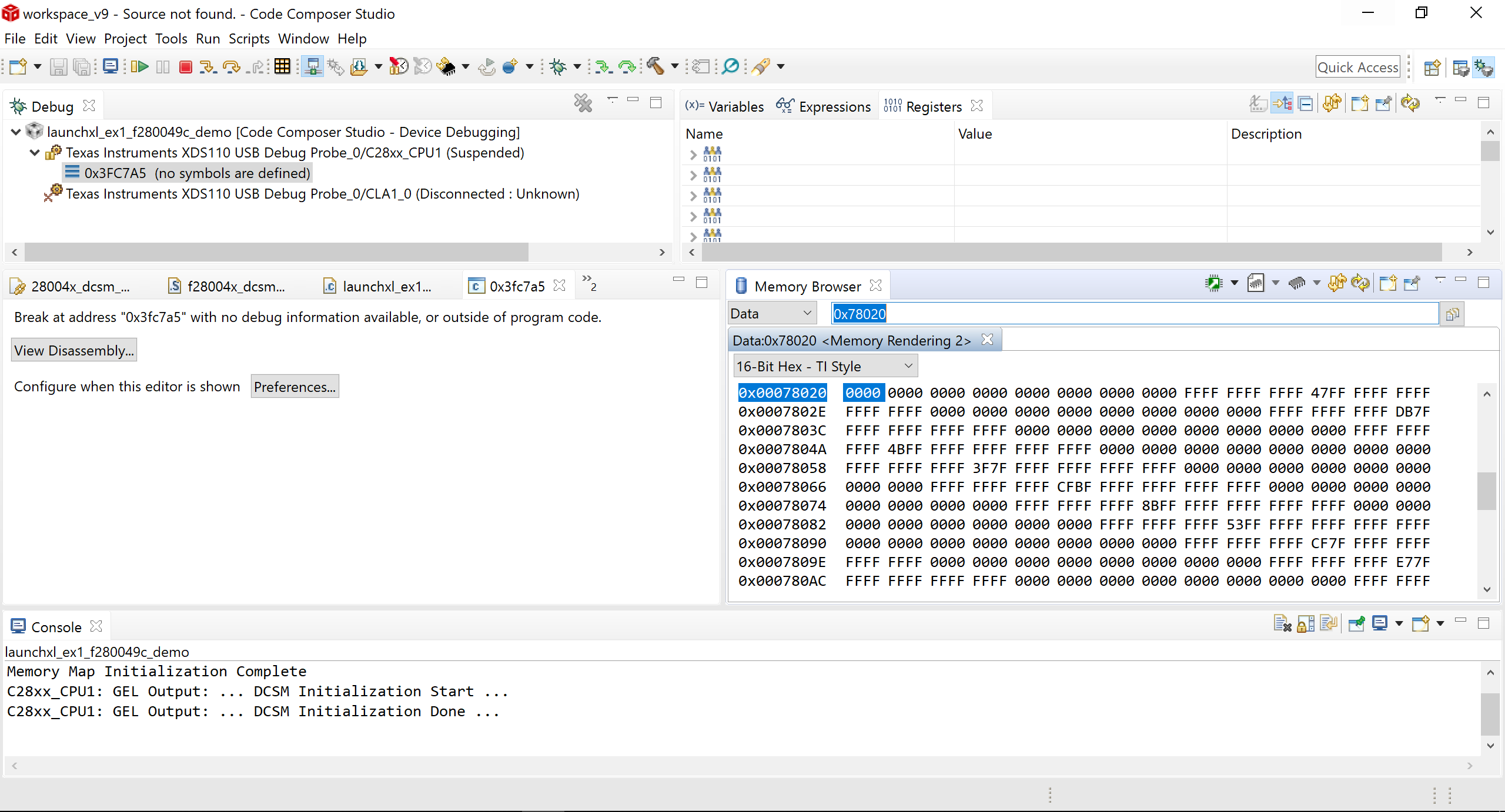
I am tring to lock F280049 with the provided asm file and cmd file but it seems goes to wrong location. Here is the asm file I modified and memory content.

It seems not to the right position, what happens here?
Attached the cmd and asm here.
CMD:
/* this linker command file is to be included if user wants to use the DCSM
 * feature on the device DCSM  means Dual Zone Code Security Module. This
 * linker command file works as an addendum ot the already existing Flash/RAM
 * linker command file that the project has.
 * The sections in the *_ZoneSelectBlock.asm source file is linked as per the
 * commands given in the file NOTE - please note fill=0xFFFF, this helps if
 * users include this file in the project by mistake and doesn't provide the
 * needed proper *_ZoneSelectBlock.asm sources.
 * Please refer to the Blinky DCSM example for proper usage of this.
 *
 * Once users are confident t`hat they want to program the passwords in OTP, the
 * DSECT section type can be removed.
 *
*/

MEMORY
{
PAGE 0 :  /* Program Memory */

   /* BANK0 */
   /* B0 Z1 OTP.  LinkPointers */
   B0_DCSM_OTP_Z1_LINKPOINTER   : origin = 0x78000, length = 0x00000C
   /* B0 Z1 OTP.  GPREG1/GPREG2 */
   B0_DCSM_OTP_Z1_GPREG         : origin = 0x7800C, length = 0x000004
   /* B0 Z1 OTP.  PSWDLOCK/RESERVED */
   B0_DCSM_OTP_Z1_PSWDLOCK	    : origin = 0x78010, length = 0x000004
   /* B0 Z1 OTP.  CRCLOCK/RESERVED */
   B0_DCSM_OTP_Z1_CRCLOCK	    : origin = 0x78014, length = 0x000004
   /* B0 Z1 OTP.  GPREG3/BOOTCTRL */
   B0_DCSM_OTP_Z1_BOOTCTRL	    : origin = 0x7801C, length = 0x000004

   /* DCSM Z1 Zone Select Contents (!!Movable!!) */
   /* B0 Z1 OTP.  Z1 password locations / Flash and RAM partitioning */
   B0_DCSM_ZSEL_Z1_P0	        : origin = 0x78020, length = 0x000010

   /* B0 Z2 OTP.  LinkPointers */
   B0_DCSM_OTP_Z2_LINKPOINTER	: origin = 0x78200, length = 0x00000C
   /* B0 Z2 OTP.  GPREG1/GPREG2 */
   B0_DCSM_OTP_Z2_GPREG	        : origin = 0x7820C, length = 0x000004
   /* B0 Z2 OTP.  PSWDLOCK/RESERVED */
   B0_DCSM_OTP_Z2_PSWDLOCK	    : origin = 0x78210, length = 0x000004
   /* B0 Z2 OTP.  CRCLOCK/RESERVED */
   B0_DCSM_OTP_Z2_CRCLOCK	    : origin = 0x78214, length = 0x000004
   /* B0 Z2 OTP.  GPREG3/BOOTCTRL */
   B0_DCSM_OTP_Z2_BOOTCTRL	    : origin = 0x7821C, length = 0x000004

   /* DCSM Z1 Zone Select Contents (!!Movable!!) */
   /* B0 Z2 OTP.  Z2 password locations / Flash and RAM partitioning  */
   B0_DCSM_ZSEL_Z2_P0	        : origin = 0x78220, length = 0x000010


   /* BANK1 */
   /* B1 Z1 OTP.  LinkPointers */
   B1_DCSM_OTP_Z1_LINKPOINTER	: origin = 0x78400, length = 0x00000C

   /* DCSM B1 Z1 Zone Select Contents (!!Movable!!) */
   /* B1 Z1 OTP.  Flash partitioning */
   B1_DCSM_ZSEL_Z1_P0	        : origin = 0x78420, length = 0x000010

   /* B1 Z2 OTP.  LinkPointers */
   B1_DCSM_OTP_Z2_LINKPOINTER	: origin = 0x78600, length = 0x00000C

   /* DCSM B1 Z1 Zone Select Contents (!!Movable!!) */
   /* B1 Z2 OTP.  Flash partitioning  */
   B1_DCSM_ZSEL_Z2_P0	        : origin = 0x78620, length = 0x000010
}

SECTIONS
{
   b0_dcsm_otp_z1_linkpointer 	: > B0_DCSM_OTP_Z1_LINKPOINTER		PAGE = 0, type = DSECT
   b0_dcsm_otp_z1_gpreg			: > B0_DCSM_OTP_Z1_GPREG			PAGE = 0, type = DSECT
   b0_dcsm_otp_z1_pswdlock		: > B0_DCSM_OTP_Z1_PSWDLOCK			PAGE = 0, type = DSECT
   b0_dcsm_otp_z1_crclock		: > B0_DCSM_OTP_Z1_CRCLOCK			PAGE = 0, type = DSECT
   b0_dcsm_otp_z1_bootctrl		: > B0_DCSM_OTP_Z1_BOOTCTRL			PAGE = 0, type = DSECT
   b0_dcsm_zsel_z1				: > B0_DCSM_ZSEL_Z1_P0				PAGE = 0

   b0_dcsm_otp_z2_linkpointer	: > B0_DCSM_OTP_Z2_LINKPOINTER		PAGE = 0, type = DSECT
   b0_dcsm_otp_z2_gpreg			: > B0_DCSM_OTP_Z2_GPREG			PAGE = 0, type = DSECT
   b0_dcsm_otp_z2_pswdlock		: > B0_DCSM_OTP_Z2_PSWDLOCK			PAGE = 0, type = DSECT
   b0_dcsm_otp_z2_crclock		: > B0_DCSM_OTP_Z2_CRCLOCK			PAGE = 0, type = DSECT
   b0_dcsm_otp_z2_bootctrl		: > B0_DCSM_OTP_Z2_BOOTCTRL			PAGE = 0, type = DSECT
   b0_dcsm_zsel_z2				: > B0_DCSM_ZSEL_Z2_P0				PAGE = 0, type = DSECT

   b1_dcsm_otp_z1_linkpointer 	: > B1_DCSM_OTP_Z1_LINKPOINTER		PAGE = 0, type = DSECT
   b1_dcsm_zsel_z1				: > B1_DCSM_ZSEL_Z1_P0				PAGE = 0, type = DSECT

   b1_dcsm_otp_z2_linkpointer	: > B1_DCSM_OTP_Z2_LINKPOINTER		PAGE = 0, type = DSECT
   b1_dcsm_zsel_z2				: > B1_DCSM_ZSEL_Z2_P0				PAGE = 0, type = DSECT
}

/*
//===========================================================================
// End of file.
//===========================================================================
*/
ASM:
;;#############################################################################
;;
;; FILE:   f28004x_dcsm_z1otp.asm
;;
;; TITLE:  Dual Code Security Module Zone 1 OTP
;;
;; DESCRIPTION:
;;
;;         This file is used to specify Z1 DCSM OTP and zone select block
;;         values to program.
;;
;;         In addition, the 60 reserved values after the zone select block
;;         are all programmed to 0x0000 as well.
;;
;; !!IMPORTANT!! The below memory sections are mapped to OTP (one-time
;; programmable) memory with the *dcsm_lnk.cmd linker command file. In order
;; to program the below memory sections, user should uncomment the .long words
;; of each section and change the value to what is desired. Additionally, the
;; corresponding section of *dcsm_lnk.cmd should no longer be labelled as a
;; dummy section. Remove ", type = DSECT" in SECTIONS from the memory section
;; that is being programmed.
;;
;;
;; !!IMPORTANT!! The "bx_dcsm_otp_z1_linkpointer" section contains the
;; Z1 LINKPOINTER which determines the location of the Z1 Zone Select block.
;; If the LINKPOINTER is changed, then the "bx_dcsm_zsel_z1_linkpointer"
;; section in the *_dcsm_lnk.cmd command linker file must also change to an
;; address decoded from the value specified in the Z1-LINKPOINTER location.
;;
;;
;; The "bx_dcsm_zsel_z1" section contains the actual Z1 Zone Select Block
;; values that will be linked and programmed into to the DCSM Z1 OTP Zone
;; Select block in OTP.
;; These values must be known in order to unlock the CSM module.
;;
;; It is recommended that all values be left as 0xFFFFFFFF during code
;; development.  Values of 0xFFFFFFFF do not activate code security and dummy
;; reads of the Z1 DCSM PWL registers is all that is required to unlock the
;; CSM. When code development is complete, modify values to activate the
;; code security module.
;;
;; ******************************WARNING***************************************
;; It is recommended not to program 0xFFFFFFFF to user OTP locations, if users
;; intend to comeback and re-program any of the bits to '0' in future. If user
;; programs 0xFFFFFFFF to any of the OTP locations then the ECC locations would
;; get programmed to a non erased state and users won't be able to comeback
;; and re-program the OTP location to another value. Please refer to DCSM
;; chapter of device TRM for more details on ECC for the locations in DCSM.
;;
;; Hence TI ships this example commenting out the initialization of all the
;; below locations.
;;#############################################################################
;; $TI Release: F28004x Support Library v1.07.00.00 $
;; $Release Date: Sun Sep 29 07:29:19 CDT 2019 $
;; $Copyright:
;// Copyright (C) 2019 Texas Instruments Incorporated - http://www.ti.com/
;//
;// Redistribution and use in source and binary forms, with or without
;// modification, are permitted provided that the following conditions
;// are met:
;//
;//   Redistributions of source code must retain the above copyright
;//   notice, this list of conditions and the following disclaimer.
;//
;//   Redistributions in binary form must reproduce the above copyright
;//   notice, this list of conditions and the following disclaimer in the
;//   documentation and/or other materials provided with the
;//   distribution.
;//
;//   Neither the name of Texas Instruments Incorporated nor the names of
;//   its contributors may be used to endorse or promote products derived
;//   from this software without specific prior written permission.
;//
;// THIS SOFTWARE IS PROVIDED BY THE COPYRIGHT HOLDERS AND CONTRIBUTORS
;// "AS IS" AND ANY EXPRESS OR IMPLIED WARRANTIES, INCLUDING, BUT NOT
;// LIMITED TO, THE IMPLIED WARRANTIES OF MERCHANTABILITY AND FITNESS FOR
;// A PARTICULAR PURPOSE ARE DISCLAIMED. IN NO EVENT SHALL THE COPYRIGHT
;// OWNER OR CONTRIBUTORS BE LIABLE FOR ANY DIRECT, INDIRECT, INCIDENTAL,
;// SPECIAL, EXEMPLARY, OR CONSEQUENTIAL DAMAGES (INCLUDING, BUT NOT
;// LIMITED TO, PROCUREMENT OF SUBSTITUTE GOODS OR SERVICES; LOSS OF USE,
;// DATA, OR PROFITS; OR BUSINESS INTERRUPTION) HOWEVER CAUSED AND ON ANY
;// THEORY OF LIABILITY, WHETHER IN CONTRACT, STRICT LIABILITY, OR TORT
;// (INCLUDING NEGLIGENCE OR OTHERWISE) ARISING IN ANY WAY OUT OF THE USE
;// OF THIS SOFTWARE, EVEN IF ADVISED OF THE POSSIBILITY OF SUCH DAMAGE.
;// $
;;#############################################################################

      .sect "b0_dcsm_otp_z1_linkpointer"
;;    .long 0x1FFFFFFF     ;B0_Z1OTP_LINKPOINTER1
;;    .long 0xFFFFFFFF     ;Reserved
;;    .long 0x1FFFFFFF     ;B0_Z1OTP_LINKPOINTER2
;;    .long 0xFFFFFFFF     ;Reserved
;;    .long 0x1FFFFFFF     ;B0_Z1OTP_LINKPOINTER3
;;    .long 0xFFFFFFFF     ;Reserved

      .sect "b0_dcsm_otp_z1_gpreg"
;;
;;    See the ROM Code and Peripheral Booting chapter of TRM for more details.
;;
;;    Below is a description of the bit fields of Z1OTP_BOOTPIN_CONFIG
;;    used by Boot ROM.
;;
;;    | Key (31-24) | BMSP2 (23-16) | BMSP1 (15-8) | BMSP0 (7-0) |
;;
;;    Below is a description of the bit fields of Z1OTP_GPREG2 used by
;;    Boot ROM.
;;
;;    | Key (31-24) | RSVD (23-8) |  RSVD (7-6) | ESP (5-4) | RSVD (3-0) |
;;
;;    .long 0xFFFFFFFF     ;Z1OTP_BOOTPIN_CONFIG
;;    .long 0xFFFFFFFF     ;Z1OTP_GPREG2

      .sect "b0_dcsm_otp_z1_pswdlock"
;;    .long 0xFFFFFFFF     ;Z1OTP_PSWDLOCK
;;    .long 0xFFFFFFFF     ;Reserved

      .sect "b0_dcsm_otp_z1_crclock"
;;    .long 0xFFFFFFFF     ;Z1OTP_CRCLOCK
;;    .long 0xFFFFFFFF     ;Reserved

      .sect "b0_dcsm_otp_z1_bootctrl"
;;
;;    See the ROM Code and Peripheral Booting chapter of TRM for more details.
;;
;;    Below is a description of the bit fields of Z1OTP_BOOTDEF_LOW used by
;;    Boot ROM.
;;
;;    | BOOT_DEF3(31-24) | BOOT_DEF2(23-16) | BOOT_DEF1(15-8) | BOOT_DEF0(7-0) |
;;
;;    Below is a description of the bit fields of Z1OTP_BOOTDEF_HIGH
;;    used by Boot ROM.
;;
;;    | BOOT_DEF7(31-24) | BOOT_DEF6(23-16) | BOOT_DEF5(15-8) | BOOT_DEF4(7-0) |
;;
;;    .long 0xFFFFFFFF     ;Z1OTP_BOOTDEF_LOW
;;    .long 0xFFFFFFFF     ;Z1OTP_BOOTDEF_HIGH

      .sect "b0_dcsm_zsel_z1"

    .long 0xFFFFFFFF     ;B0_Z1OTP_EXEONLYRAM
    .long 0xFFFFFFFF     ;B0_Z1OTP_EXEONLYSECT
    .long 0xFFFFFFFF     ;B0_Z1OTP_GRABRAM
    .long 0x55555555     ;B0_Z1OTP_GRABSECT Select all Sector in Zone 1

    .long 0x11223344     ;B0_Z1OTP_CSMPSWD0 (LSW of 128-bit password)
    .long 0x11223344     ;B0_Z1OTP_CSMPSWD1
    .long 0x11223344     ;B0_Z1OTP_CSMPSWD2
    .long 0x11223344     ;B0_Z1OTP_CSMPSWD3 (MSW of 128-bit password)

      .sect "b1_dcsm_otp_z1_linkpointer"
;;    .long 0x1FFFFFFF     ;B1_Z1OTP_LINKPOINTER1
;;    .long 0xFFFFFFFF     ;Reserved
;;    .long 0x1FFFFFFF     ;B1_Z1OTP_LINKPOINTER2
;;    .long 0xFFFFFFFF     ;Reserved
;;    .long 0x1FFFFFFF     ;B1_Z1OTP_LINKPOINTER3
;;    .long 0xFFFFFFFF     ;Reserved

      .sect "b1_dcsm_zsel_z1"
;;    .long 0xFFFFFFFF     ;Reserved
;;    .long 0xFFFFFFFF     ;B1_Z1OTP_EXEONLYSECT
;;    .long 0xFFFFFFFF     ;Reserved
;;    .long 0xFFFFFFFF     ;B1_Z1OTP_GRABSECT

;;    .long 0xFFFFFFFF     ;Reserved
;;    .long 0xFFFFFFFF     ;Reserved
;;    .long 0xFFFFFFFF     ;Reserved
;;    .long 0xFFFFFFFF     ;Reserved

;;----------------------------------------------------------------------

;; For code security operation,after development has completed, prior to
;; production, all other zone select block locations should be programmed
;; to 0x0000 for maximum security.
;; If the first zone select block at offset 0x10 is used, the section
;; "dcsm_rsvd_z1" can be used to program these locations to 0x0000.
;; This code is commented out for development.

;;        .sect "dcsm_rsvd_z1"
;;        .loop (1e0h)
;;              .int 0x0000
;;        .endloop


;;#############################################################################
;; End of file
;;#############################################################################
Thanks
Sheldon