This thread has been locked.

If you have a related question, please click the "Ask a related question" button in the top right corner. The newly created question will be automatically linked to this question.

TMS320F28335: C2000™ microcontrollers forum

Part Number: TMS320F28335
Other Parts Discussed in Thread: C2000WARE, PGA113

Dear Support, i have an issue regarding F28335 ADC noise.
I use a TMS320F28335PGFA (lqfp 176 pin package) and I have some noise when reading ADC.
I use the same component in different boards, with different power supply, different voltage reference (external on one board and internal on the others).
I bought also a board from a supplier available on the market just to check the noise and compare to my ones.

Here the reference: solectroshop.com/product-eng-1437-DSP-Learning-Board-ZQ28335-DSP28335-Microprocessor-TMS320F28335.html

The result is that there is always noise of about +/- 30-40 bits when I measure a fixed dc voltage.
I have also checked ripple on power supply, but it is not measurable with 10mV/div scope, so it should be below 1-2mV.
I tried also to change sample rate, from 250/500Ksps to 6.25Msps, but noise seems always present.
I tried also to divide analog and digital ground in one board or using just a common ground on another, but there is not a big difference.
The only situation that helps is put a small capacitor very close to a/d converter analog input. My standard values for RC input filter are 47 ohms series resistor and 3,3nF ceramic capacitor, just to realize a small RC low pass filter.
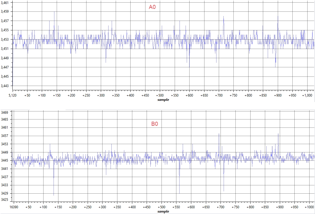
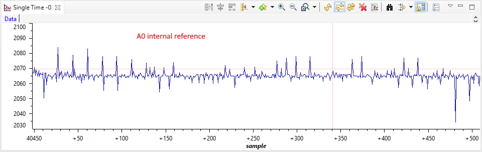
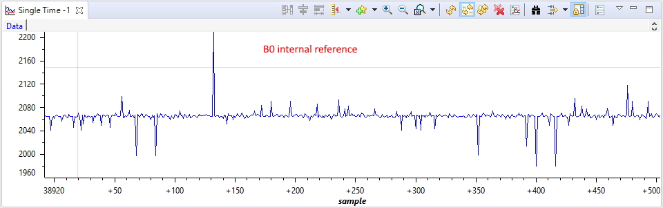
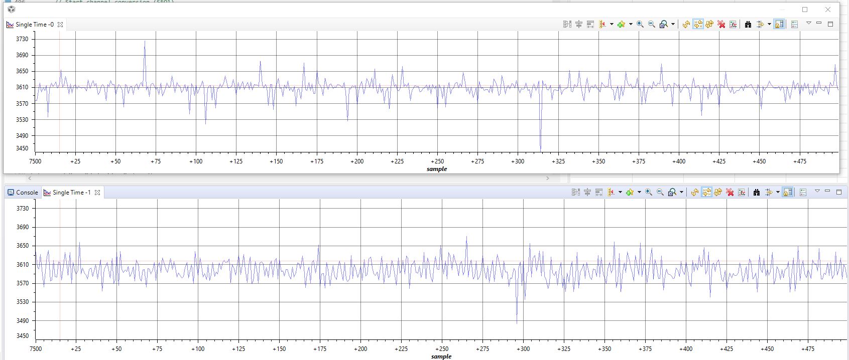
Here attached some screenshot of acquired signal at different sampling rate and with different boards layout, trace on the top is for analog input A0, trace bottom for analog input B0.

DSP Learning Board ZQ28335 6.25MSps

DSP Learning Board ZQ28335 250KSps

My board 1 common ground internal ref.  6.25 MHz

My board 1 common ground internal ref.  500Ksps

I gave a look to the following tickets but without any real advantage.

e2e.ti.com/.../924719.aspx
e2e.ti.com/.../937894.aspx
e2e.ti.com/.../940713.aspx

The only one board I test with effectively no noise (just some bits) is the TMS320F28335 control card plus base board rev 2.2.
I gave a look to schematic of the board but I did’t find differences that justify this difference about noise. The only one difference is the package of the chip: BGA on control board, LQFP for all other ones. So my question: could be a reason for why BGA has less noise? Is there a control card with 176 pin LQFP package?
Have you any other suggestion?

Take into account that on m,y boards:
1) ground is a ground plane on top layer plus inner layer connected with several vias,
2) power supply is not noisy or with ripple. I tried also to use the control board 1,9 and 3,3V power supply and routing it on my board by disconnecting my ones but nothing changes.
3) On my board input B of multiplexer seems always a bit noisy than input A.
4) I have mounted several boards with several F28335 production batches without find differences.
5) ADCREFP and M are connected to 2,2uF ceramic X5R capacitor connected to ground plane; ADCRESEXT connected to ground via 22Kohm resistor.
6) Analog supply are decoupled by different capacitors: 2,2uF, 0,1uF and 22pF for both 1,9 and 3,3V.

In the past I did’t need high speed analog conversion so I did averaging for noise reduction but now I need 1Msps to 6.25Msps on 2 channels so I cannot do averaging.
Any other suggestion will be appreciated, I’m in the designing phase of a new board.
Thanks in advance.
Roberto

  • Hi Roberto -

    If I were faced with the same issue, I would try to post-process the ADC results through an FFT to see if I could ascertain what spectral components are present in your signal; it kind of looks like there's some periodicity to it.  If you have spurs at certain frequencies, that would point to a deterministic cause (e.g. coupling from a nearby trace or bus) rather than something random.  Are your ADC inputs in close proximity to any switching supplies, or does your sampled circuit share a common return path with one?  How about nearby clocks?  Have you sampled around your board with a sensitive EMI sniffer probe?

    I would also explore using an external, good-quality voltage reference, unless you're specifically going for ratiometric sampling (where the sensor is also powered by the voltage you're using as a reference, nulling out the effect of any noise common to both).

    Good luck to you!

    Josh

  • Dear Josh. thanks for quickly reply.
    I did an FFT af an acquired sample buffer to find if there is any spurious dominant frequency but i didn't find anything.
    About layout take into account that i have same issue on at least 3 different board layout. I use the DSP in different products ad i tried a test  A/D acquisition firmware on all the boards i have with more or less same result.
    Normally my analog input is not ratiometric with reference voltage, but in one board i used an external reference the also is used as common reference for analog section and it is quite a simple board with just insulated inputs and outputs and some communication ports. I tried also to do not initialize any other internal DSP peripherals, just the A/D one just to avoid any interference, but nothing changes.
    If you have any other idea is well appreciated.
    Thanks anyway
    Roberto

  • Your confusion and consternation make a lot of sense Roberto - I would be similarly frustrated in those circumstances.  I wish I had something else to offer, but I don't have any direct experience with that part to fall back on.

    One final thought: you mentioned your application requires a fast sampling speed and that you can't tolerate averaging; I think I would try to use a fast median filter with a small window size, because that filter type has the advantage of passing a step function while still removing noise.  I have no idea how much horsepower you have available for that and how it would affect your throughput; perhaps if your C2000 part has a CLA available, you could program it to independently accomplish this with little or no impact to your main thread.  I realize this solution (if indeed it is one) doesn't address whatever root cause is at play here.

    I'm grasping at straws now, so I'll refrain from further speculation and hope someone from TI contacts you soon.

    Josh

  • Roberto,

    I found a socketed LQFP eZdspF28335 board here and ran the adc_seq_ovd_test example from C2000Ware using a precision reference voltage as the input to the ADC.  The example continuously stores ADC samples into a 1024 result buffer at 8.25MSPS.  My separate runs for channels A0 and B0 are below.

    The bulk of the conversions are relatively well behaved with some notable excursions here and there. I did not see any signal conditioning (filtering) on the ADC channels so there is room for improvement. The performance should also improve for a soldered device vs a socketed device.

    Can you try running the adc_seq_ovd_test example on your boards to see if the spread is similar? This will at least help to eliminate the possibility of a software configuration issue.

    -Tommy

  • Dear Tommy, here below you can find the result of the adc_seq_ovd_test example running on my board at 8,33Msps. Input signal was the output of analog amplifiers chain (2 in cascade) without any input signal biased at 1,5V by external reference.

    It seems to me that there is more noise than the one in your example, but take into account that i have an analog amplifier as input. I didn't do a test with external references as low noise input bias because I should have to cut some PCB tracks and manually add wiring.
    I tried also to do acquisition by selecting external references, but more or less result is the same.
    Anyway it seems to me that in both acquisition, mine and yours, there is more noise on B0 channel than in A0, and "sometimes" on both channel, there is some spikes the goes above the "standard" amount of noise. These spikes seems involve only just one sample reagrdless sample rate.
    Probably i will add a fast median filter as kindly suggested by Josh (thanks!) to remove these spikes, because it is not clear for me the cause.
    Any other suggestion will be appreciated.
    Roberto
  • Roberto,

    Can you confirm that the amplifier circuit bandwidth is high enough to fully charge the S+H capacitor within the ACQ_PS window?  For example, with a 25MHz ADC clock, you would want a bandwidth greater than 25MHz / (ACQ_PS+1).

    An alternate approach would be to use a very large input capacitor (greater than 2^14 * 1.64pF = ~27nF) to realize charge sharing between the input capacitor and the S+H capacitor.  The amplifier would need to recharge the input capacitor between samples.

    We have observed situations where GPIO pin toggling can increase the noise floor of the ADC.  For exampling, enabling XCLKOUT or ongoing emulation JTAG activity.

    I would not expect external reference mode to make a significant difference in this case.

    -Tommy

  • Tommy,

    my amplifier is a PGA 113 from TI, I'm doing noise test check with gain=1. The last acquisition at 8,33Msps was done with ACQ_PS=1.

    Here below an extract of PGA113 data sheet

    The output of PGA si routed to the F28335 ADCIN thru a 47Ohm series resistor ad a 1nF parallel capacitor to ground.

    Then, I have added an extra 2,2nF capacitor closed to ADCIN pin ad Analog ground of F28335, this helps to reduce noise.  

    So at the input of ADC I have a RC low pass filter.

    Do you think i need to increase this capacitor to 27nF? This will reduce the passband frequency of the RC low pass filter.    

    Take into account that spikes are present even at lover sampling rate, like 250Ksps as in my previous post, where ACQ_PS has an higher value.

    Regards

    Roberto

  • Roberto,

    I flipped through the PGA113 datasheet and it looks to be more in line with a precision amplifier rather than a high-speed amplifier.  The datasheet itself uses a 500kHz ADC as an example, which I think is below your target rate.  Is there any opportunity to try a higher speed amplifier?

    We recently added some RC selection guidelines to the ADC chapter of the F2806x TRM.  The ADC architecture is different, but the RC selection guidelines would apply to the F2833x ADC as well.

    For the current PGA113 implementation, you might be able to improve the results by maximizing the ACQ_PS window through a combination of the ACQ_PS register setting and the ADC clock dividers where you can still achieve your desired sampling rate.  Then update your RC component values using the High Bandwidth equations from the F2806x TRM.

    The 27nF capacitor recommendation came from the Low Bandwidth equations, but it sounds like this may not be desirable for your system.  It may be worth a try just to see if the conversions improve.

    -Tommy

  • Roberto,

    Were you able to see any improvements?

    -Tommy

  • Here attached you can find two acqusitions, made with ACQ:_PS at maximum value: 15.

    The zoom scale for A0 acquisition is not the best, but it seems to me that more or less spikes are around +/- 10 to 20 bits, while for channel B0 are significantly higher.

    Unfortunately I cannot change analog front end, maybe i can reduce the 47ohm series resistor..
    Anyway it is not clear for me why the same analog signal is very quiet when i do an acquisition with the TMS320F28335 control card plus base board, with same software settings.
    And why B0 still remain more noisy than A0.
    I think that at the moment i'll use only A0 mux by routing my 2 channels on it and i'll apply a fast median filter just to remove the 1 sample spike.
    Roberto


  • Roberto,

    I am also puzzled by the noise on your B-channels.  I hope that your proposed mitigation techniques will be sufficient.

    I will close this thread for now; feel free to reopen it if you want to take another look at the issue.

    -Tommy