This thread has been locked.

If you have a related question, please click the "Ask a related question" button in the top right corner. The newly created question will be automatically linked to this question.

CCS/TMS320F28377D: Extended Wait Mode and the EM1WAIT Pin

Part Number: TMS320F28377D

Tool/software: Code Composer Studio

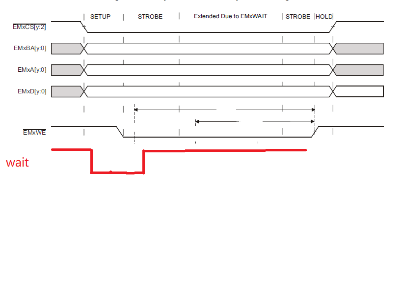
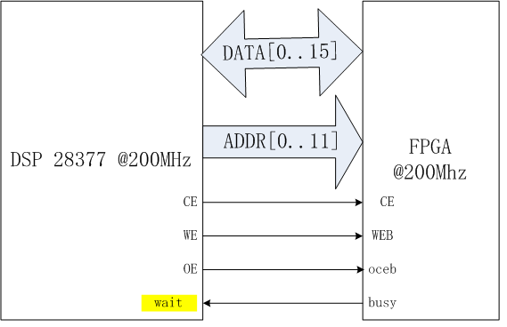
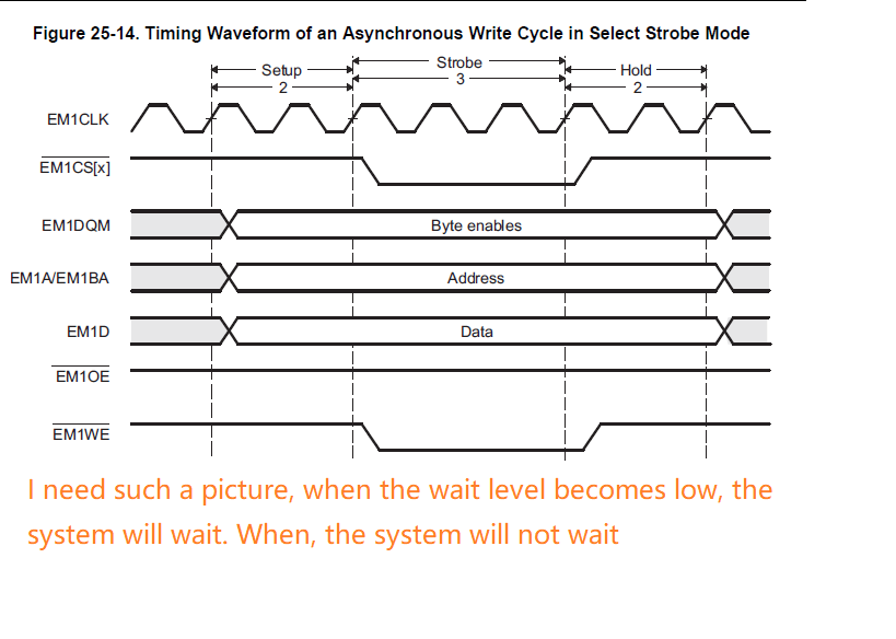
I use 28377 EMIF to connect Dual port RAM for asynchronous communication. The busy pin of Dual port RAM is connected to theEM1WAIT Pin of 28377. Because the manual only describes the wait mode in words, and there is no sequence diagram. I hope you can draw a brief sequence diagram to let me understand the correct sequence logic of 28377's EMIF bus when the wait pin gets low.Because I have observed that when the busy signal jumps to a low level, the EMIF bus does not wait. So I expect to know when the busy level becomes low, and then the EMIF bus will wait.

//Configure the access timing for CS2 space
//
Emif1Regs.ASYNC_CS2_CR.all = (EMIF_ASYNC_ASIZE_16 | // 16Bit Memory
// Interface
EMIF_ASYNC_TA_2 | // Turn Around time
// of 2 Emif Clock
EMIF_ASYNC_RHOLD_2 | // Read Hold time
// of 2 Emif Clock
EMIF_ASYNC_RSTROBE_8 | // Read Strobe time
// of 8 Emif Clock
EMIF_ASYNC_RSETUP_2 | // Read Setup time
// of 2 Emif Clock
EMIF_ASYNC_WHOLD_2 | // Write Hold time
// of 2 Emif Clock
EMIF_ASYNC_WSTROBE_8 | // Write Strobe time
// of 8 Emif Clock
EMIF_ASYNC_WSETUP_2 | // Write Setup time
// of 2 Emif Clock
EMIF_ASYNC_EW_ENABLE | // Extended Wait
// Enable.
EMIF_ASYNC_SS_DISABLE // Strobe Select Mode
// Disable.
);

Emif1Regs.ASYNC_WCCR.bit.WP0=0;
//The max wait time for (max_ext_wait + 1) * 16 clock cycles before the busy signal goto high
Emif1Regs.ASYNC_WCCR.bit.MAX_EXT_WAIT=0x80;
//enable AT,LT interrupt,disable WR interrupt
Emif1Regs.INT_MSK_SET.bit.AT_MASK_SET=1;
Emif1Regs.INT_MSK_CLR.bit.WR_MASK_CLR=1;
Emif1Regs.INT_MSK_SET.bit.LT_MASK_SET=1;

  • Hi,

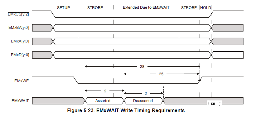
    Datasheet has figure 5-22 and 5-24 which explains when wait signal should get asserted/de-asserted. As per that, min setup time for WAIT to be asserted is 4E+20 ns which translate to 40ns if EMIF clock is configured as 200MHz (wrt end of strobe phase). As per your configuration, READ STROBE is set to 8 which is 40ns so it'll not meet the spec. You need to increase the strobe time to use the wait feature.

    Regards,

    Vivek Singh

  • Thank you very much for your reply!I've seen these  figures.I still have two questions.

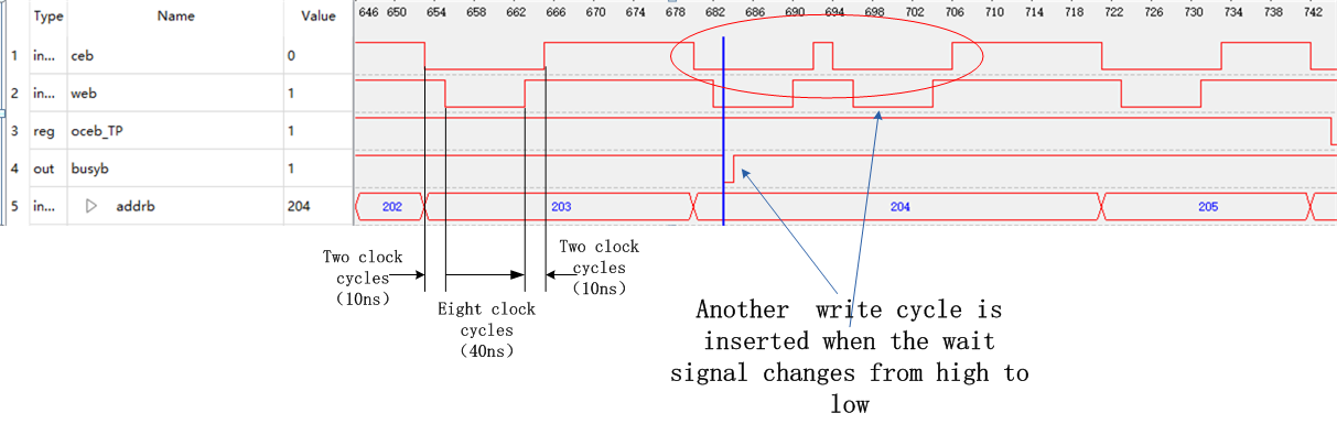
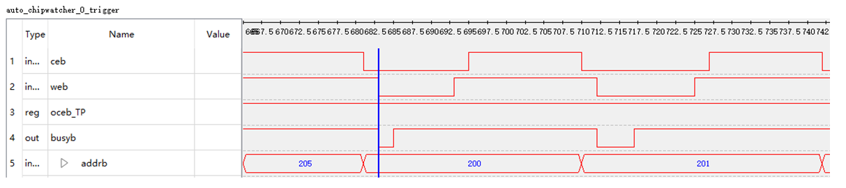
    1.I use FPGA to simulate dual port RAM for asynchronous communication. We can see that a wait signal is generated (see the figure below).  it takes the same time(t1=t2) to write the cycle as when wait pin is high level and   low level. Why are there no more clock cycles inserted in the write cycle when wait pin is low level?At the beginning of the page, I have attached the program code that contains register settings.Please see if these settings are correct.

    2.Suppose that the wait signal occurs at the position in the figure below, the wait signal becomes low before  WE, will the WE signal still be generated?

  • Hi,

    On point #1

    I am not sure from this figure if you are meeting the timing (setup and hold) for WAIT signal. Can you provide the timing for t2 and from blue line (toggle of WAIT) to de-assertion of WE signal? Can you extend the WAIT for longer time to see if that helps (just to make sure no issue with configuration).

    On point #2

    Yes, WE will be generated

    Regards,

    Vivek Singh

  • I'm sorry for the delay in replying to you.In order to understand the role of the wait pin, we build the following system.

    1.The ideal Asynchronous Memory Write Timing is shown in the figure below

    But in the picture below we can see that when the WAIT signal becomes low, sometimes the EMIF bus can insert another write cycle, and sometimes it will not insert another write cycle.(The figure below shows obtaining bus timing from JTAG of FPGA. This timing chart is consistent with the bus timing configured by dsp28377, so it can be considered as correct.)

    We can also observe that sometimes DSP will not insert more write cycles.In the figure below, we can see that the time spent in a write cycle with a wait signal is the same as that spent without a wait signal.

    In either case, it is not consistent with the standard time sequence described by datasheet.

    2.The standard timing of the reading cycle is shown in the figure below.

    We see when the wait signal changes from high level to low level, 28377 does not extend the reading cycle time, nor insert one more reading cycle.

    Why the timing inconsistency with the manual?

  • Hi,

    Wait signal will not insert another write cycle. It only extends the ongoing access if asserted at correct time. Can you check your assembly code and see if there are two back to back access there? Also can you have the wait signal extended for a long duration (instead of a small pulse) and see if that extends the WRITE and READ cycle.

    Regards,

    Vivek Singh

  • 1. When the received wait signal is low, 28377 actively sends out two write cycles, which has nothing to do with program coding. The WE signal is 28377 output. 2. In the bottom picture, in the reading cycle, the wait signal has been generated long enough, almost as long as the OE signal, but we still can't see that 28377 has inserted the wait time.

  • Hi,

    1. When the received wait signal is low, 28377 actively sends out two write cycles, which has nothing to do with program coding.

    That should not happen. We do not see this in our simulation. Can you provide the timing in that waveform as well.

    2. In the bottom picture, in the reading cycle, the wait signal has been generated long enough, almost as long as the OE signal, but we still can't see that 28377 has inserted the wait time.

    Can you increase the READ STROBE by another 2 cycle in configuration? The minimum setup time itself is 40ns so your strobe time has to be more than that.

    Regards,

    Vivek Singh

  • Hi,

    Did you try any further experiments as suggested in last post?

    Regards,

    Vivek Singh

  • There are other important tasks at hand and the test needs to be postponed.

  • Ok, please let us know when you have time to look into this again.

  • I am closing this post now. Please start a new post when you have time and provide the link of this one in that post.

    Regards,

    Vivek Singh