This thread has been locked.

If you have a related question, please click the "Ask a related question" button in the top right corner. The newly created question will be automatically linked to this question.

TMS320F280049: Schematic design for F280049 56pin

Part Number: TMS320F280049

Dear Champions,

Currently I'm designing 280049 56pin's schematic, and have several questions about it, can you please give your hand on it?

1. If the internal ocsilater was used, how to handler the X1(pin 41)? 

2. How to handler the PGAx_GND if I didn't use the PGA feature?

3. For JTAG program interface, is it neccessary to pull up JTAG pins with resistor? If it is, what resitor value you recommend?

4. What's your recommendations of handling the other unused anlog input pins and GPIOs?

5. In lauchpad and control card schematic, I see that a ferrite bead was used to connect 3V3_A 3V3_D with 3V3, is this ferrit bead neccessary? Because my team didn't have used this compoenent before, what your suggestions of the replacement? please help provide a suggestion circuite if you have a replacement.

6. What your recommendations of connecting VSS and VSSA? I see those 2 ground were connect together in control card and lauchpad.

  • Hi Jack,

              Please see comments below:

    1. If the internal ocsilater was used, how to handler the X1(pin 41)? 

    [JC] - Connect X1 to GND if using internal oscillator for clock and to ensure that the internal oscillator is stable over time, please follow the recommended guidelines in choosing external cap on VDD since on the 56pin device, the VREG is on by default.

    2. How to handler the PGAx_GND if I didn't use the PGA feature?

    [JC] - Tie this to VSSA.

    3. For JTAG program interface, is it neccessary to pull up JTAG pins with resistor? If it is, what resitor value you recommend?

    [JC] - Please follow the recommended data sheet values for JTAG pull-up in section 5.8.5 "Emulation/JTAG" - 4.7k for TMS pin and 10k for TDI and TDO.

    4. What's your recommendations of handling the other unused anlog input pins and GPIOs?

    [JC] - Please follow datasheet recommendations in table 4-10 "Connections for Unused Pins" for unused analog and GPIO channels.

    5. In lauchpad and control card schematic, I see that a ferrite bead was used to connect 3V3_A 3V3_D with 3V3, is this ferrit bead neccessary? Because my team didn't have used this compoenent before, what your suggestions of the replacement? please help provide a suggestion circuite if you have a replacement.

    [JC] - Ferrite bead is recommended for applications that are critical to EMI reduction.  Use the ferrite beads if the circuit will be subject to high frequency environment.  Placing the ferrite bead on the 3V3 rails would offer high frequency noise suppression on the 3V3 rails and reducing the impact of the noise going into the F280049 through the supply rails.  It is probably best that you first asses what high frequency signals will be present on the system that you are designing for.  It might be enough just to have a 0.1uF shunt cap on the 3V3 rail close to the IC and to boost that, you can add a ferrite bead too.  Again, all these considerations would be dependent on the environment where the circuit will be used and what will be available beads that meet the noise suppression that you need.  There is a good reading article on this that is worth considering for your design.

    6. What your recommendations of connecting VSS and VSSA? I see those 2 ground were connect together in control card and lauchpad.
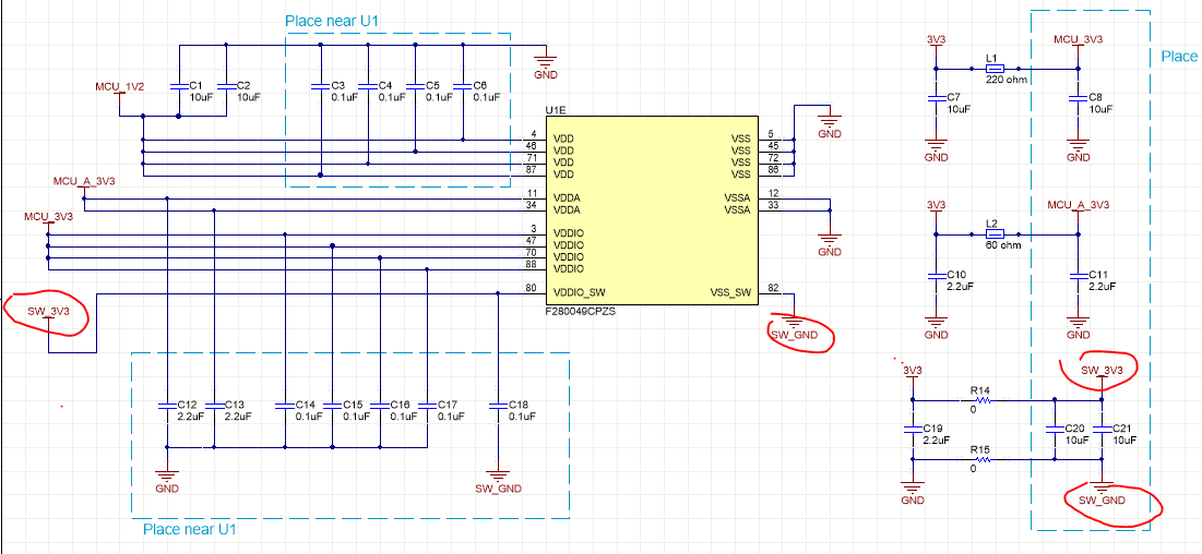
    [JC] - Have separate plane for VSS where you ground all digital related signals then another ground plane for analog signals, then at one point, connect both VSS and VSSA grounds together.

    Best regards,

    Joseph

  • Hi Joseph,

    Thanks for your detail comments abou it.

    6. What your recommendations of connecting VSS and VSSA? I see those 2 ground were connect together in control card and lauchpad.
    [JC] - Have separate plane for VSS where you ground all digital related signals then another ground plane for analog signals, then at one point, connect both VSS and VSSA grounds together.

    [Jack Tan] - I see the control card and lauchpad are used the single pannel in PCB, why don't seperate it and connect those 2 grounds at one place?

    7. [Jack Tan] - XRSn, the datasheet recommends to tie it to VDDIO with a 2.2K resistor, but the control card and lauchpad are connected to +3V3, what's your recommendations?

    8. [Jack Tan] Regarding to VSS_SW and VDDIO_SW, I see VSS connect VSS_SW with 0 ohm resistor,  and +3V3 connect VDDIO_SW  with 0 ohm resistor. But the datasheet recommends to tie to VSS and VDDIO if using internal VREG, what's your suggestions about this?

  • Hi Jack,

    Please see my comments in red.

    6. What your recommendations of connecting VSS and VSSA? I see those 2 ground were connect together in control card and lauchpad.
    [JC] - Have separate plane for VSS where you ground all digital related signals then another ground plane for analog signals, then at one point, connect both VSS and VSSA grounds together.

    [Jack Tan] - I see the control card and lauchpad are used the single pannel in PCB, why don't seperate it and connect those 2 grounds at one place?

    [JC] - Best practice layout design calls for separate ground planes for digital and analog blocks.  This would minimize the coupling of digital circuit blocks and clocks that often require switching from logic 0 to logic 1 usually at higher speeds to the analog blocks, like the ADC for instance if precision conversions are required.  Launchpads and control cards are development boards where users can start creating SW and can use these as basis for designing HW as well, but due to the limited space, having separate ground planes is not practical.  If your application requirements are met with the current layout of the Launchpad and control card having just one ground plane, then you can adapt it as well.  This requirement really will be dictated by your system needs.

    7. [Jack Tan] - XRSn, the datasheet recommends to tie it to VDDIO with a 2.2K resistor, but the control card and lauchpad are connected to +3V3, what's your recommendations?

    [JC] - Not sure what the concern is here.  In both Launchpad and control card, I see that there is a 2.2k pullup to 3V3 on the XRSn pin.  Note that VDDIO is also connected to 3V3.

    8. [Jack Tan] Regarding to VSS_SW and VDDIO_SW, I see VSS connect VSS_SW with 0 ohm resistor,  and +3V3 connect VDDIO_SW  with 0 ohm resistor. But the datasheet recommends to tie to VSS and VDDIO if using internal VREG, what's your suggestions about this?

    [JC] - I guess your question is why are there 0ohm resistors on VSS_SW and VDDIO_SW to VSS and VDDIO respectively  These were added in Launchpad and control cards for flexibility in case there is an future experiment with DCDC that requires a different connection to these pins.  For your application, you can omit these 0ohm resistors and connect VSS_SW to GND and VDDIO_SW to VDDIO.

    Regards,

    Joseph

  • Hi Joseph,

    Thanks for your detail infomation.

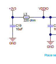
    Regarding to item 7, please see below screen shot  about +3.3V and VDDIO, there is a ferrit bead that connect the +3V3 and VDDIO, I agree that the voltage should be same for 3.3V and VDDIO, but the noise level might have some differences.

    In contorl card and lauchpad, the resitor on XRSn pin is pull up to +3V3, but the datasheet recommends it should be pull up to VDDIO. What's your suggestions about XRSn's pull up resistor connection? +3V3 or VDDIO?

    Happly Thanksgiving Day in advance.

  • Hi Jack,

    Thank you!  In this case, you would want XRSN pull up to be in VDDIO side since the ferrite bead makes VDDIO less noisy.  You want to have a clean and stable high level signal on XRSn to avoid spurious reset.

    Best regards,

    joseph

  • Hi Joseph,

    Thank you, it's clear.

  • Hi Joseph,

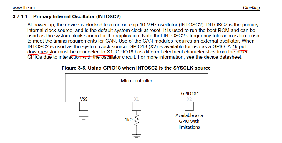
    One more questions about the X1 connection if internal oscillator was used, I see that TRM suggestion it should be pull down to VSS with a 1k resistor, but datasheet suggest tie to VSS directly, my qestions is that is the 1K pull down resistor neccessary?

  • Hi Jack,

    The 1k pull-down is only necessary if using X2 as GPIO18.

  • Thanks for this info.