This thread has been locked.

If you have a related question, please click the "Ask a related question" button in the top right corner. The newly created question will be automatically linked to this question.

TMS320F280049: CMPSS query to implement peak current mode control of a 4 switch 3-phase interleaved bi-directional buck boost converter

Part Number: TMS320F280049

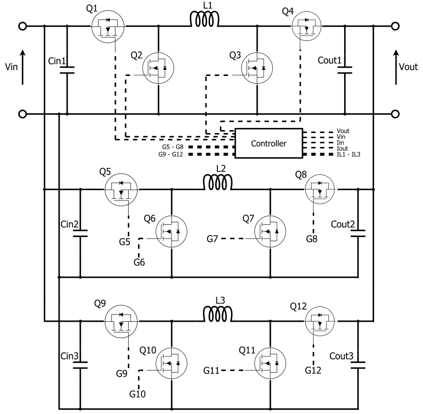
I'm using the TMS320F280049 for a 4 switch 3-phase interleaved bi-directional converter as shown in the diagram. I have questions regarding the CMPSS module to implement peak current mode control by using the inductor currents. The inductor currents range from 0V to 3.3V where 0V = -110A, 3.3V = +110A and 1.65V = 0A. The input to the positive terminal of the comparator are each inductor phase currents.
(1) There is a point during operation when Buck and Boost are required, i.e. all MOSFET's are switching. I need to connect 2 comparators in parallel to facilitate the Buck and Boost sections of the converter as the reference to the comparator is the sum of the ramp signal plus the output of a digital compensator. Each compensator of the Buck and Boost will have different coefficients and hence require two comparators. Can you confirm that it's not possible to implement Buck and Boost with one comparator module?
(2) How can I facilitate (1) in the reverse direction given the inductor current is negative with respect to the 0A (1.65V) reference point? Would I need to invert the output of the digital compensator for either the Buck or Boost and then sum this with the rising ramp signal?


  • Tony, 

    Can you provide a diagram as to how you see the PWM changing for buck and boost switches with the inductor current?

    IN general i feel this is not something you can handle with one CMPSS.

    For 2, as you are aware we have only falling RAMP generator. Hence if you really want PCMC in reverse direction you will need to inverter the sensing on another channel and then use another CMPSS.

    -Manish 

  • The switching PWM scheme for buck-boost switching and inductor current is described on page 17 in LT8705 and page 4 in TIDU638.

    My apologies, I made an error with my first post and the RAMP is indeed falling. I'm assuming by your comment 'inverter the sensing on another channel' that you're suggesting I invert the inductor current signal (with respect to 1.65V) in hardware and then process this signal on another CMPSS module?

  • Tony,

    None of those two references use PCMC, I am unable to understand your requirements with PCMC as applied to buck and boost. (Note I am the author of TIDU638)

    For simplicity, let's assume you have just a bi-directional buck. For this the challenge will be the ramp is only falling and hence if you really need to do PCMC in the reverse direction and will like to use slope compensation then you will need to invert this using an opamp inverter circuit and feed it to a different CMPSS when the power is really in the opposite direction. 

    WIth the detail provided so far I cannot visualize the PCMC with buck and boost, so please provide a diagram with the exact waveform needed with slop compensation, to offer an evaluation. 

  • Manish,

    Just to clarify, the LT8705 operates using inductor current mode control. It measures the peak of the inductor current waveform in the boost region and the valley of the inductor current waveform in the buck region. 

    What specifically can you not visualise Peak Current Mode Control (PCMC) in buck and boost. These are very common architectures and very well documented. SLVA636 discusses PCMC for a Boost Converter which I found very helpful.

    Thank you for clarifying the additional hardware required in making my system operate in forward and reverse directions. Can you confirm the following for a 4 switch 3-phase interleaved bi-directional buck boost converter:

    (1) For forward direction current flow, I will need 2 comparators for each phase. A total 6 comparators.

    (2) In the reverse direction, I will need 2 comparators for each phase with changes to the hardware. A total of 6 comparators.

    From what I can gather, the TMS320F280049 is not an ideal choice (correct me if I'm wrong) for this application given the ramp signal is only falling and the ramp can only be applied to the negative terminal of the comparator.

    (3) Can you think of any possible way to implement the above in software i.e. without the additional inductor phase current inversion hardware? The only way I can think of (which requires additional hardware) is to analog OR the positive and inverted negative inductor current. This signal is then connected to the positive terminal of two comparator modules of the TMS320F280049 to process Buck and Boost. I would require 6 comparators in total.

  • Tony,

    What is missing from your description is a detailed diagram of what you want, i understand the reference document but they are not exactly what you want or asking for.

    People have been sucesfull is using CLA for slope compensation by emulating the ramp in software, this was before slope compensation was available in hardware on F28035. 

    http://centaur.reading.ac.uk/31751/1/Microcontroller%20Based%20Peak%20Current%20Mode%20Control%20Using%20Digital%20Slope%20Compensation%20-%20Hallworth%202012.pdf 

    https://e2e.ti.com/cfs-file/__key/communityserver-discussions-components-files/171/Digital-Peak-Current-Mode-Control-With-Slope-Compensation-Using-the-TMS320F2803x.pdf

  • Manish,

    Thank you for the useful links. The TMS320F280049 has 2 DAC's in total and from what I gather, I would need to connect the output of the DAC to the CMPSS module. I will need a total of 6 DAC's to fulfil my requirements of a 3-phase interleaved Buck and Boost. I don't believe this is a feasible solution for my application.

    In response to your vague request of a detailed diagram of what I want, I will implement something similar to the following which is an extract from Microcontroller Based Peak Current Mode Control Using Digital Slope Compensation. The difference with my application is that I'm measuring the inductor current and replacing the diode with a MOSFET.

  • F280049 has 2 DAC that are external to the MCU,

    We have additional DACs inside the CMPSS which which are 2 DACs for each module. 

    The paper mainly focusses on the ramp signal being generated by software instead of RAMP being available in the CMPSS module itself. 

    Also the reason i requested for the information is because you have four switches and I wanted to comprehend the changes needed for that in the PWM if I was advising you on the forum.  

  • Manish,

    If I understand correctly, I can use the internal DAC of the CMPSS module to generate a rising and falling ramp signal?

  • Tony, 

    As I indicated above, the CMPSS DAC has an inbuilt RAMP generator which is only falling. I have recommended to you two methods as work around

    1. Use a rectified current signal such that ramp is only falling. 

    2. Or, Write to DAC directly using SW bypassing the internal Ramp, we even have DMA access to CMPSS module which can be used to write the values that the hardware integrated ramp will write.

    -Manish 

  • Manish,

    I would like to proceed with Option 2 which is to write directly to the DAC using software bypassing the internal Ramp. Can you suggest any examples or code that I can use to realise this requirement.

  • Hi, Sorry for my delay in the reply. I do not have any ready example for this available unfortunately.