This thread has been locked.

If you have a related question, please click the "Ask a related question" button in the top right corner. The newly created question will be automatically linked to this question.

TMS320F28377D: MAXIMUM CLOCK SETTING at 200Mhz

Part Number: TMS320F28377D
Other Parts Discussed in Thread: C2000WARE

Hi Guys, just a quick question. I've set my F28377D clock speed to 200Mhz and it really doesn't seem to be actually running at 200Mhz.

I've used other MCU's at 200Mhz and my F28377D seems and feels a lot slower. My F28377D is mounted on a control card with docking station  VR4.1.

The F28377D's default OSC is 10Mhz so I've set the multiplier to 20 and all dividers to divided by 1. Enabled the new clock speed.

If I raise the multiplier the F28377D does run faster but that means I'm overclocking it right?

Do I need to set waitstates for speeds at 200Mhz or is there other settings I have to set to get maximum 200Mhz speed from my C2000 CPU in the F28377D.

All settings is set from Assembler and not C. I'm an assembler programmer.

Thanks guys and hope to hear from you soon.

Pete

  • Hi Pete,

    First, just wanted to understand how the 200MHz internal clock was measured on the F28377D control card.  Did you connect a scope and brought out the SYSCLK externally and measured it, or was there some sort of a code running (exact same code running on another MCU) and timed the execution?  If so what code was this?

    Can you try setting the multiplier by 40, instead of 20?  This will produce an internal VCO clock of 400MHz, which is around the nominal rating of the internal VCO.  100MHz VCO is at the very low end of the spec.  Set the dividers to 2 so SYSCLK will be at 200MHz.

    Regards,

    Joseph

  • Hi Joseph, thanks for the info. I was just looking at my assembly codes SYSCLK settings and I've set the CPU clock to use the external OSC and didn't realise it.

    Let me check it out and get back to you but I will try your 400Mhz / 2 for the SYSCLK.

    Thanks Joseph.

    Pete


  • Hi Pete,

    Did you get a chance to check out the clock settings and validate that SYSCLK is running at 200MHz?  Let me know if you still have issues with clocking.

    Best regards,

    Joseph

  • Hi Joseph, sorry I was away. I've just got back and tried changing the clock to 400Mhz / 2.

    I've written a small assembler program to put 16bit data onto PORTB. I'm just sending 65535 and then sending 0 so the port is toggling.

    I measured the toggling time and my OSC reads.... ready for it... 1.92Mhz. LOL. Something has to be wrong.

    I left the clock at 400Mhz with divide by 1 and my scope now reads 3.85Mhz. That's better but still way to slow.

    The manual says maximum speed of the IO PORTS is 25Mhz and I can only get 3.85Mhz. 

    Here's my clock settings in assembler.

            EALLOW			; ALLOW PROTECTED REGISTERS TO BE ACCESSED.
    	MOVL XAR7,#CLKSRCCTL1	;CLKSRCCTL1 = 0
    	MOVW AL,#0		; INTERNAL CLOCK INTOSC2
    	MOVW AH,#0
    	MOVL *XAR7,ACC
    
    	MOVL XAR7,#SYSPLLMULT	;SYSPLLMULT
    	MOVW ACC,#40
    	MOVL *XAR7,ACC
    
    	MOVL XAR7,#SYSCLKDIVSEL
    	MOVW AL,#0
            MOVW AH,#0
    	MOVL *XAR7,ACC
    
    	MOVL XAR7,#SYSPLLCTL1	;ENABLE NEW CLOCK
    	MOVW ACC,#3
    	MOVL *XAR7,ACC
    
    __SPEED_TEST:
    	EALLOW
    	MOVL XAR7,#GPBDIR	; PORTB TO OUTPUT
    	MOVW AL, #65535	
    	MOVW AH, #65535
    	MOVL *XAR7,ACC
    	EDIS
    
    	MOVL XAR7,#GPBDAT
    
    SPEED_TEST_LOOP:
    	MOVL XAR6,#65535
    	MOVL *XAR7,XAR6
    	NOP
    	MOVL XAR6,#0
    	MOVL *XAR7,XAR6
    	NOP
    	BF SPEED_TEST_LOOP,UNC

    I've tried overclocking it as well and the fastest speed I can get from the IO PORT is 4.1Mhz. 

    Anything above that and the chip doesn't run.

    I've read the manual over and over and I believe I've set up the PLL but if you have any other ideas

    please let me know.

    Thanks Joseph and waiting for your reply.

    Peter

  • Hi Peter,

    The definitive way to determine what frequency the device is operating at would be to enable XCLKOUT and measure the frequency on the XCLKOUT pin.  Note that there is a divider by default (which you will want to keep) since the max GPIO frequency is I believe 50MHz.

    Using an ePWM module is another possibility. 

    Overall you want to take the SW execution speed variable out of the picture.    

  • Hi Devin, thanks for the reply.

    I've setup the F28377D to a 10" LCD using the lower half (16bits) of PORTC and clearing the screen with colour and clearing the whole screen takes about 1 second. I've set the sysmult to 40 with no dividers and still it's too slow. I've used the same LCD with a PIC32 running at 200Mhz and the screen cleared with colour almost instantly like it should. That's why I'm thinking my F28377D is not running as fast as it should. The IO Ports on the F28377D max speed is 25Mhz as it states in the manual but I just can't even get close to that speed. Maximum speed I can get is 4.1Mhz. Maybe my F28377D is faulty but it seem to run code ok, but slowly.

    I'll try setting up the clock in C, maybe I'm missed some settings in assembler. Oh I'll test the XCLKOUT as you suggested as well.

    Thanks again Devin

    Peter

  • Hi Peter,

    Its a good idea to enable XCLKOUT to get the actual CPU clock rate, as Devin has pointed out.  Looking at your ASM code, i'm not sure that the PLL configuration is done properly.  Anyway for your reference, i've deconstructed the C code for setting up the PLL (using INTOSC2 as clock):

    // use INTOSC2 to clock PLL

    ClkCfgRegs.CLKSRCCTL1.bit.INTOSC2OFF=0; // Turn on INTOSC2
    ClkCfgRegs.CLKSRCCTL1.bit.OSCCLKSRCSEL = 0; // Clk Src = INTOSC2
    ClkCfgRegs.CLKSRCCTL1.bit.XTALOFF=1; // Turn off XTALOSC

    //
    // Bypass PLL and set dividers to /1
    //
    ClkCfgRegs.SYSPLLCTL1.bit.PLLCLKEN = 0;

    //
    // Delay of at least 120 OSCCLK cycles required post PLL bypass
    //
    asm(" RPT #120 || NOP");
    ClkCfgRegs.SYSCLKDIVSEL.bit.PLLSYSCLKDIV = 0;

    //
    // Turn off PLL
    //
    ClkCfgRegs.SYSPLLCTL1.bit.PLLEN = 0;
    asm(" RPT #20 || NOP");

    //
    // Write multiplier, which automatically turns on the PLL
    //
    ClkCfgRegs.SYSPLLMULT.all = ((fmult << 8U) | imult);

    //
    // Wait for the SYSPLL lock counter
    //
    while(ClkCfgRegs.SYSPLLSTS.bit.LOCKS != 1);

    // Set the divider

    ClkCfgRegs.SYSCLKDIVSEL.bit.PLLSYSCLKDIV = divsel;

    //

    // Enable PLLSYSCLK is fed from system PLL clock
    //
    ClkCfgRegs.SYSPLLCTL1.bit.PLLCLKEN = 1;

    We determined that the NOPs above are required for proper operation so you would need to insert these to your code as well. 

    Regards,

    Joseph

  • Hi Joseph, thank you for the info above. I have to say it's exactly the same as my PLL setup code except for the delays.

    I inserted the delays+100 more NOP's to wait extra time and set the multiplier to 40 and then tested the speed of PORTA with my scope.

    4.1Mhz was the highest speed. If I set the multiplier to 43 I get 4.6Mhz but thats the top speed limit. Any setting higher than 43 and the F28377D won't run.

    So at this stage I'm thinking that the F28377D PORTS CAN NOT run at 25Mhz like the hardware manual states.

    Can you do me a favour? Can you or a TI technician test the data rate on PORTA in C or assembler with a scope at and let me know what speed they can get. 

    Thanks again for all your help on this.

    Peter

  • Hi Peter,

    As part of the digital/analog coupling performance analysis of the F28377D ADC module, i have ran several evaluations where ADC is operating while GPIOs are toggling from minimum to maximum speed.  I am able to toggle the GPIO ports at max rate of 25MHz rate so i know this works.  I'm still doubting if PLL is properly configured with your code.  To validate this, can you try bringing out the CPU SYSCLK on the XCLKOUT pin by adding this to your code:

    MOVL XAR7,#CLKSRCCTL3
    MOVW AL,#2 ; CPU1 SYSCLK out of XCLKOUT pin
    MOVW,AH,#0
    MOVL *XAR7, ACC
    XCLKOUTDIV is div by 8 by default but if you want to want to be sure, add in this code as well:
    MOVL XAR7,#XCLKOUTDIVSEL
    MOVW AL,#3 ; 3=div 8, 2=div 4; 1=div2; 0=div 1 
    MOVW,AH,#0
    MOVL *XAR7, ACC
    XCLKOUT pin in F28377D would be ball A16 in the 377 BGA package, pin 140 in the 176 QFP package or pin 81 in the 100PZ package.  Hope you have access on XCLKOUT pin.  If the PLL is configured correctly, you should measure 25MHz on the XCLKOUT pin with a properly configured 200MHz SYSCLK.
    The sequence of PLL setup in the F28377D is  critical so i'd recommend to follow the flow as described in the C code i pasted above.  Also, i do not see the lock counter being polled in your ASM code as soon as the multiplier value is written to SYSPLLMULT (this is also  critical).  You should poll SYSPLLSTS (LOCKS bit) to ensure it is '1' before enabling PLLCLKEN.  I also do not see XTALOFF bit set in your ASM code for register CLKSRCCTL1.
    Regards,
    Joseph
     
  • Hi Joseph. *** HAPPY NEW YEAR *** :)

    The XCLKOUT pin on my F28377D control card is not accessible. I checked the PDF on the pinout of the Control Card Docking Station Version [R4.1] my F28377D control card is using and there is no XCLKOUT pin so I can't check the clock speed via that pin.

    I added the delays where you said in my code for PLL lock and others and it worked fine. I even read the PLL Lock register and it = 1 meaning PLL Locked successfully.

    Can you do me the favour as I asked in my last reply. I need to test my code on your F28377D to compare with my speed test results.

    Can you clock your F28377D at 200Mhz and with a scope test the speed of raw data on PORTA. Just setup the clock your way and use my code (below) to test the RAW data rate on PORTA and please let me know your results. Heres my code again.

    Again, than you so much for your help on this.

    ; SPEED TEST ON PORT A
    			EALLOW
    			MOVL XAR7,#GPADIR		; SET PORTA TO OUTPUT
    			MOVL XAR6,#GPADAT
    			MOVW AL,#65535
    			MOVW AH,#65535
    			MOVL *XAR7,ACC
    			EDIS
    
    TEST_LOOP:
    			MOVW AR2,#65535              ;16 bits only
    			MOVW *XAR6,AR2
    			MOVW AR3,#0
    			MOVW *XAR6,AR3
    			BF TEST_LOOP,UNC

  • Hi Joseph, I just found this inside this file F2837xD.SysCtrl.c from C2000ware.

    // Initialize the PLL control: SYSPLLMULT and SYSCLKDIVSEL.
    //
    // Defined options to be passed as arguments to this function are defined
    // in F2837xD_Examples.h.
    //
    // Note: The internal oscillator CANNOT be used as the PLL source if the
    // PLLSYSCLK is configured to frequencies above 194 MHz.
    //
    // PLLSYSCLK = (XTAL_OSC) * (IMULT + FMULT) / (PLLSYSCLKDIV)
    //

    This is probably why my PLL clock is not running as fast as it should. Maximum clock using the internal OSC is 194Mhz.

    Pete.

  • Hi Pete,

    Happy new year too!!

    Because of the +/-3% tolerance of the internal oscillator, that note was added taking into account that worse case INTOSC2 frequency would be lower by 3% of the target (10MHz*(0.97)*IMULT/PLLSYSCLKDIV = 194MHz).  Should still be OK to clock using INTOSC2, only that 200MHz cannot be guaranteed because of INTOSC tolerance.

    I tried your exact ASM code that loops writing '1' and '0' to 16 GPIO ports of port A and i'm able to see GPIO transitions of 18.2MHz.  See scope capture below:

    The MOV and branch instructions take up CPU cycles so you would not be able to attain maximum GPIO rate.  If you wanted to attain 25Mhz or higher rate on the GPIO, you can use the CLA instead to update GPIODAT and free up CPU cycles for this task.

    I think you still have an issue with your clock setup.  You might not be configuring CPU1 to run at ~200MHz SYSCLK.  The setup i have configured for the above exercise is using INTOSC2 with a multiplier of 40 and a PLL divider of 1 (div by 2) to produce ~200MHz SYSCLK.

    Best regards,

    Joseph

  • Hi Joseph, thank you so much for running my code. Now I know for a fact that either my PLL is not being setup properly or my control card is faulty. 

    I'll go over the PLL setup in the Technical Reference Manual step by step, write the code, test that the registers are actually changing and go from there.

    Thank you so much for helping me out of this. 

    Peter :)

  • Hi Peter,

    Your're welcome.  In the meantime, let me close this thread.  If you have still have issues with your PLL set up, please post it in the forum and we will do our best to work with you with your debug needs.

    Regards,

    Joseph

  • Hi Joseph I've setup the XCLKOUT pin73 on my F28377D and the INTOSC1 and INTOSC2 is clocking at 9.22Mhz on my scope.

    I set CLKSRCCTL3 to 0 (PLLSYSCLK) and my scope read 0. I guess my PLL setup is wrong.

    Can you give me a step by step line by line in C to correctly setup the PLL and I will translate it to Assembler.

    I know you game me the C code above but is that 100% correct? Because I tried that and it didn't work.

    If my PLL is not running then why does my F28377D run faster when I raise the PLL multiplier? Strange.

    Peter

  • Hi Joseph, PLL is working now. I rewrote the assembler code from your C listing above and this time it's working.

    I setup the XCLKOUT via mux and the PLLCLK now reads 200Mhz. Multiplier is set to 43 / 2 on my system.

    I ran the scope on my PORTA toggle assembly program and now it reads 4.9Mhz. How did you get 25Mhz on your PORTA?

    Could there be a fault with my F28377D card?

    Please let me know.

    Thanks Joseph

    Peter.

  • Hi Peter,

    Good to know you have the PLL working and are able to observe internal clock from the XCLKOUT pin!   I did not do anything else with your asm code.  I used it as it is, which basically is a loop that just writes 0xFFFF and 0x0 to GPIO port A after the PLL is set.  I doubt that is is a HW issue, and before we conclude that, here are a couple of things that you might want to check:

    - Can you set the multiplier to 40/2.  This way you will get the SYSCLK in spec at 200MHz?  215MHz (43/2) is outside of the device's operating range.

    - What was the value set for XCLKOUTSEL when bringing out the internal clock to XCLKOUT pin?  By default, this will bring out PLLRAWCLK, not the CPUCLK (which will be the clock used when writing PORTA values to GPIO).

    - What is the value of SYSPLLCTL1.PLLCLKEN (should be '1') and has enough NOPs been added after setting this '1'?  This is key as CPU will still be clocking off of internal oscillator 1 (which is also ~10MHz) before PLLCLKEN is set to '1' and writing this bit will require several INTOSC clock cycles.

    Best regards,

    Joseph

  • Hi Joseph, Thanks for the info. :). I've done what you've said. Changed the clock back to 40 / 2.

    I also read the CLKSRCCTL3 register to see what value PLLRAWCLK equals and it equals 0. What value is it suppose to be?

    One more thing, I had an idea that there was another clock running the IO PORTS like the other MCU's we have here but I couldn't find any info about an IO PORTS clock in the TRM.

    Now that you've mentioned that the PLLRAWCLK is used to write to the PORTS I'm thinking thats the clock I've been looking for. At the moment it's probably set with a divider of 40 which kind of makes sense because 200/40 = 5Mhz BUT as usual I could be wrong and your the expert on this.

    I've looked in the TRM and there's only very little info about the PLLRAWCLK. It doesn't say anything about clocking IO PORTS at all. Well I can't find any info.

    Please let me know how to change the PLLRAWCLK to get 25Mhz on my PORTS.

    Thank you so much for your help so far, you would not believe how much I appreciate it. I almost gave up and was going to use another MCU for our product but don't worry, We're sticking with TI.

    Peter 

  • Hi Peter,

    You are welcome, and glad to work with you on this issue.

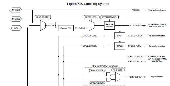
    The IO port transactions are clocked off of the CPU1 clock.  Just to give an idea, let us take a look at the clock tree of the F28377D device (snippet from the TRM):

    What you were probably monitoring is PLLRAWCLK in XCLKOUT as that is the default setting.  PLLRAWCLK probably has not propagated to CPU1 SYSCLK in your case.  Hopefully the diagram helps with your debug, if you want to take that path ... or try to use the PLL code below that I have translated from the C2000Ware C version to assembly.  The ASM code is below:

    ;/*
    ; * pllset.asm
    ; *
    ; *  Created on: Jan 7, 2020
    ; *      Author: a0844182
    ; */
    ;***************************************
    ; Equates table                      ***
    ;***************************************
    
    CLKSRCCTL1					.set	05D208h
    CLKSRCCTL3					.set	05D20Ch
    SYSPLLCTL1					.set	05D20Eh
    SYSPLLMULT					.set	05D214h
    SYSPLLSTS					.set	05D216h
    SYSCLKDIVSEL				.set	05D222h
    XCLKOUTDIVSEL				.set	05D228h
    GPCMUX1						.set    007C86h ; GPIOC (for GPIO73 mux selection for XCLKOUT)
    
           .def _Set_pll
    
            .global  __Set_pll
    _Set_pll:
    	EALLOW
    
    	;ClkCfgRegs.CLKSRCCTL1.bit.OSCCLKSRCSEL = 0; //Clock source = IntOsc2
    	;ClkCfgRegs.CLKSRCCTL1.bit.INTOSC2OFF   = 0; //Internal oscillator2 turned on
    	;ClkCfgRegs.CLKSRCCTL1.bit.XTALOFF	   = 1; //External oscillator / Crystal turned off
    
    	MOVL XAR7, #CLKSRCCTL1
    	MOVW ACC, #16
    	MOVL *XAR7, ACC
    
            MOVL XAR7, #SYSPLLCTL1
            MOVL XAR6, #SYSPLLMULT
            MOVL XAR5, #SYSPLLSTS
            MOVL XAR3, #SYSCLKDIVSEL
    
           ;ClkCfgRegs.SYSPLLCTL1.bit.PLLCLKEN = 0;
            ;asm(" RPT #20 || NOP");
            TCLR *XAR7, #0
            RPT	#20||NOP
    
    SlipDetect:
    	MOV	@AR4,#5
    Relock:
    	;ClkCfgRegs.SYSPLLCTL1.bit.PLLEN = 0;
            ;asm(" RPT #20 || NOP");
            TCLR *XAR7, #0
            RPT	#20||NOP
            ;//
            ;// Write multiplier, which automatically turns on the PLL
            ;//
            ;ClkCfgRegs.SYSPLLMULT.all = ((fmult << 8U) | imult);
            MOV	ACC, #40
            MOVL *XAR6, ACC ; write multiplier, this automatically enables PLL
    check_lock:
            TBIT *XAR5, #0
            SB check_lock, NTC
            BANZ Relock,AR4--  ; lock for 5 times
    
            ; program PLL divider
            MOV ACC, #1
            MOVL *XAR3, ACC
    
           ;//
           ;// Enable PLLSYSCLK is fed from system PLL clock
           ;//
           ;ClkCfgRegs.SYSPLLCTL1.bit.PLLCLKEN = 1;
           ;    asm(" RPT #20 || NOP");
    
           TSET *XAR7, #1
           RPT #20 || NOP
    
           ; check for PLL SLIP condition
           TBIT *XAR5, #1
           SB SlipDetect, TC
    
    ; At this point, PLL should be set correctly. Add code to bring CPU SYSCLK to XCLKOUT pin just for debug purposes
    ; Remove below code after debug so GPIO73/XCLKOUT will not become an unneccesary noise source
    
    		MOVL XAR7, #CLKSRCCTL3
    		MOVW ACC, #2				; bring out CPU1 SYSCLK
    		MOVL *XAR7, ACC
    
    		MOVL XAR7, #GPCMUX1
    		MOVW AL, #0000h          ;  mux selection for XCLKOUT on GPIO73
    		MOVW AH, #000Ch
    		MOVL *XAR7, ACC
            LRETR
    
    ;============
    

    I've checked this out and am able to see the correct CPU1 SYSCLK of 200MHz (25*8).  Setting up the PLL on the F28377D is not as straightforward as
    writing to the PLL and SYSTEM registers.  The PLL needs to be enabled/disabled for at least 5x and once the PLL is locked, the SLIP bit has to be monitored
    as well.  Moreover, writing the bits of the SYSPLLCTL1 register requires some extra NOPs.  I have implemented most of these critical PLL settings in the
    ASM code.

    Let me know if this works for you.

    Regards,
    Joseph

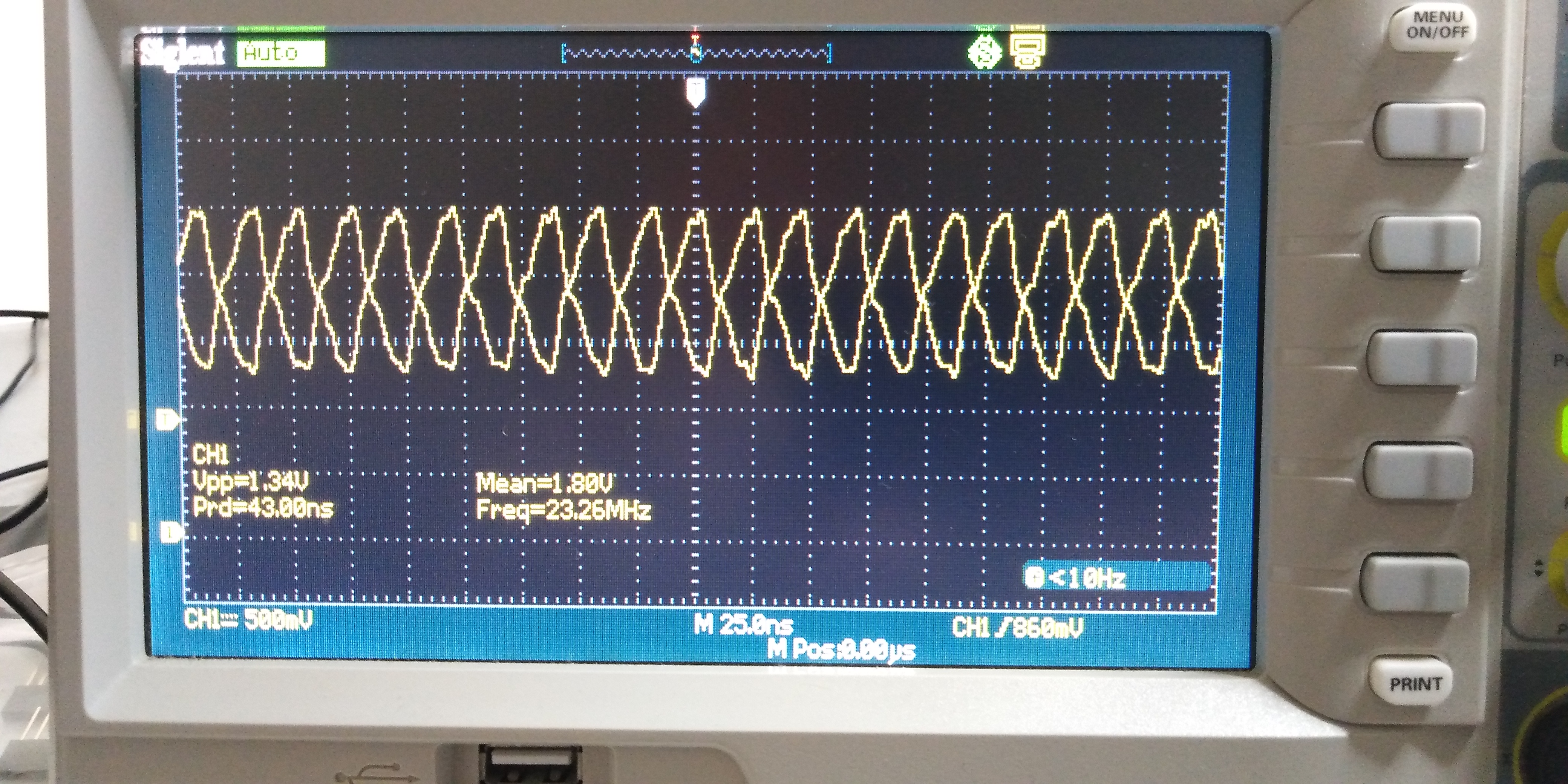
  • Hi Joseph, thanks for the ASM code. I commented my PLL code out and inserted your code in and build and downloaded the code to my F28377D control card . Checked XCLKOUT GPIO73 and my scope says 23.26Mhz. Something is not right thats for sure. 

    Peter

  • Hi Peter,

    The default XCLKOUT divider is /8, so it seems like things are working correctly.

    Joseph's last post accounts for this:

    I've checked this out and am able to see the correct CPU1 SYSCLK of 200MHz (25*8).

    And a further back post from him is a little more explicit:

    If the PLL is configured correctly, you should measure 25MHz on the XCLKOUT pin with a properly configured 200MHz SYSCLK.

  • Hi Peter,

    How fast is the GPIO toggling with this PLL set up?  Are you still getting only up to 4MHz toggles?  Also seems like you are running the code out of out of flash and not RAM for this debug, is it correct?  If running off of flash, have you configured the waitstates properly?  This will affect the speed of the data update for the GPIO port.

    Regards,

    Joseph

  • Hi Joseph, I've just tested the raw speed of PORTA with your PLL settings and now my scope reads 2.31Mhz. Thats slower than my PLL setting of 4.1Mhz.

    So if I use your PLL settings in our commercial product, 32bit parallel communication with other F28377D's will be as fast as a 1980's home computer. Blood Hell.

    You mentioned am I running it from flash. Yes we have to because we do need the FULL 1MB flash memory for our firmware.

    Waitstates will only delay the CPU 1 to 3 clocks and won't effect the IO speed that much, not 22Mhz. You said you tested your PORTA and the speed was 25Mhz using my assembly code after you setup the PLL to 200Mhz. Why am I not getting that 25Mhz. 2.3Mhz is a joke, its to slow. Our product will crawl and not sell.

    Do you think it's the waitstates now?

    Peter

  • *** UPDATE ***

    Hi Joseph, The default waitstates setting is 0xFh, no wonder the F28377D was running slow. Other MCU's at 200Mhz seemed to me to be a lot quicker.

    OK, I've set the wait-states to bit 9 because the F28377D would not run with BIT8 only set so I've set waitstates to BIT 9.

    I then tested the speed of PORTA and it said 10Mhz. YAY !!!! I almost fell off my chair. LOL, But still not 25Mhz like you reached.

    Then I found the DATACACHE and PREFETCH registers.

    Default value for BOTH of these is 0 = OFF. So I turned them both ON and now I'm getting 14.71Mhz on PORTA. Getting closer to 25Mhz.

    Can you think of anything else to set to get my ports to 25Mhz speed?

    I'm so Sorry about the last message, I was a little upset.

    Peter

  • Hi Peter,

    As i have stated earlier when i ran your PORTA ASM code, i'm only able to get as high as 18.2MHz toggle (also visible in the scope capture i sent).  This is not a limitation of the IO, but because of the MOV and branch instructions.  Here's a breakdown of your ASM loop and the associated CPU cycles:

    TEST_LOOP:
            MOVW AR2,#65535  ; 1 cycle
            MOVW *XAR6, AR2  ; 1 cycle
            MOVW AR3,#0      ; 1 cycle
            MOVW *XAR6, AR3  ; 1 cycle
            BF TEST_LOOP,UNC ; 7 cycles since branch is always taken

    Total CPU cycles for the above transactions is 11.  Multiply this by 5nS CPU period (200MHz CPU clk) and this will give a total GPIO period of 55ns or 18.18MHz toggle rate.

    To attain the highest possible toggle rate on the GPIO when doing our digital-analog crosstalk evaluation on the ADC module, we had to use the GPIOs as EPWM pins and toggled them as PWM pulses with faster rates (even in excess of 25MHz).  GPIO0 to 23 have mux functions that will allow you to use them as EPWM pins but GPIO24-31 does not have EPWM functionality.

    Per datasheet spec, you need to set the flash wait states to 3 since you are running the CPU at ~200MHz.  Probably best to put your GPIO switching code to RAM (even if your code is executing off of flash, but still configure your waitstate to 3) through  the  C function memcpy at the start of your code just to avoid the flash wait state issue:

    memcpy(&RamfuncsRunStart, &RamfuncsLoadStart, (size_t)&RamfuncsLoadSize);

    Regards,

    Joseph

  • Hi Joseph, Ah I see what you're saying. You tested the port speed using PWM, yep that explains the high speed toggle rate. I'll be using PORTA as a 32bit communication bus and needed it to be as fast as possible using the CPU. Ok, DMA should reach the data rate you reached reading from an internal ram buffer, that  would be even faster than the CPU at sending raw data to the IO port. You mentioned using the CLA as well so I'll delve into that one too.

    Thank you again for the help on the PLL. It was a little stressful. lol. :)

    Thanks Joseph and have a great day.

    Peter

  • Hi Peter,

    You're welcome.  Yeah, agree with you on the PLL.  We actually have an errata published on the PLL due to a start up issue and the fix is to re lock it a couple of times (at least 5x) and monitor for slip condition.   We made the changes to our PLL initialization routines in C2000Ware to address this errata.  If you decide to use the F28377D, just be sure to use the asm I sent for the PLL setting as this takes care of the errata.

    Agree with you with the DMA updates for GPIO data to port A if you are using this as a 32-bit port.  This will be the fastest way to send data to the port.

    Best regards,

    Joseph

  • Hi Joseph, just one last question. I'm curious which one would be quicker?

    32bits DMA data transfer on PORTA at 18Mhz or SPI 16bit data modein Hi_SPEED at 50Mhz?

    Peter

  • Hi Peter,

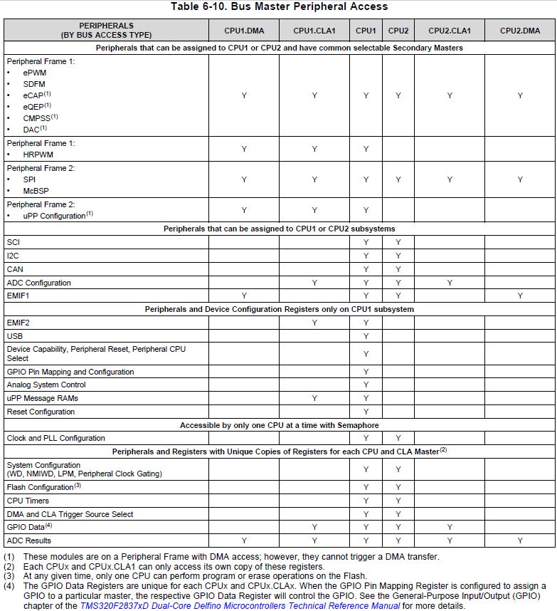
    Just realized DMA does not have access to GPIO Data on F28377D per table below from DS:

    Regards,

    Joseph

  • Hi Joseph, LOL :) Would you believe it ! ok, so DMA is out of the question then.

    Would you think SPI at 16bits data HISPEED 50Mhz transfer would be quicker than 18Mhz 32bit PORTA data transfer?

    Peter

  • Hi Peter,

    I think the GPIO data transfer will be much faster. Assuming you will be stuck with CPU  GPIO data writes since DMA is out of the equation (:, your GPIO write routine will only take 9 cycles per data update (MOVL of data to ACC[1], MOVL of ACC to GPIODAT[1] and branch[7] until all of the data are transferred) which is closer to 22MHz (45ns).  I think it will be a bit faster than your original asm routine that was writing 0xFFFF and 0x0000 back to back to the GPIO port as that required 11 cycles to complete. 

    In 50MHz HS MODE SPI, you will have your 32bit data in (20ns SPICLK)*32 or 640ns, much longer than the GPIO method.

    Regards,

    Joseph