This thread has been locked.

If you have a related question, please click the "Ask a related question" button in the top right corner. The newly created question will be automatically linked to this question.

TMS320F28376S: ADC Acquisition Window Duration

Part Number: TMS320F28376S


Dear Sir ,

we are using the 28376S chip in one of our product under development , and has some issue / questions regrading ADC Acquisition time .

1. the ADC-A is set to work in frequency of 50Mhz  (the C28x is working on 200Mhz) , Acquisition time is time to  500ns  (i have tried also 1000ns)

2. we have set 4xSOC (0..4) to Sample   specific Analog inputs (3,2,5,4,0)  - the trigger for the SOC0-4 are from PWM1 (e.g EPMSOCA in frequency of 20Khz)

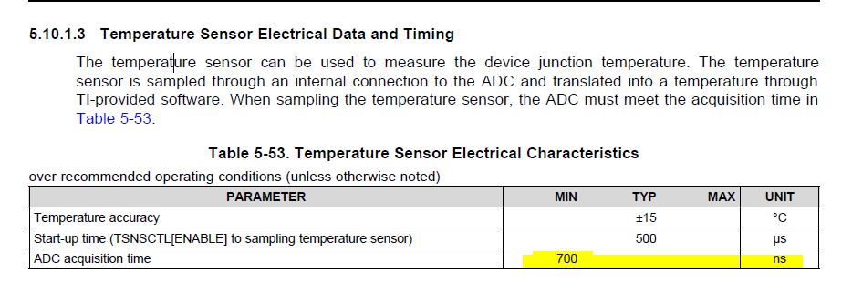
3. we have defined in addition  SOC15 to sample Internal temperature (e.g CHSEL=13), the trigger is from software every ~100ms

a. the issue we are facing is that every ~100ms (the internal temperature measurement) there is some influence  on  SOC0  (which sample right after SOC15 ) , the SOC0 is connected to 0v .

the SOC0 vary around +15 ADC points , if we stop the sample on SOC15 , there is no issue , can you advice on this issue  ?

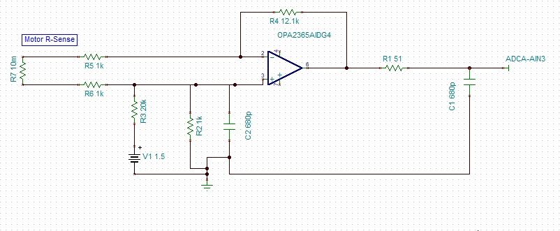
b.regarding  ADC Acquisition time  if we have on the analog pin  RC filter of RS=220 Ohm and CS=680ns  the Acquisition time according to the document will be ~ 880ns  

is it correct , or we have miscalculate ?

c. what can additionally cause influence between sequential sampling  (e.g. SCO0 influence SOC1 , SOC1 influence SOC2  )

we are suspecting that it is due to sequential sampling  and not noise , please your opinion ?

  • Hi Eyal,

    Yes, typically the impact from one sample to the subsequent sample would be due to inadequate S+H time on the subsequent channel.

    Are you sure that the 220 ohm + 680pF RC is the only impedance seen by the input?

    What is the bandwidth of the driving op-amp?  You can find a calculation for the necessary BW in the resources here: https://training.ti.com/ti-precision-labs-adcs-introduction-sar-adc-front-end-component-selection?context=1139747-1128375-1139106-1128643

    The other thing that the SW force could affect is the timing/order of the samples.  You could add the temp-sensor sample to the ePWM driven samples to get the timings consistent.  

  • Hi Devin ,

    Thank you For the Quick Response , i did try modified various  Such as ACQ Time , ADC Frequency , even SET SOC15 (Internal Temperature ) to by trigger by PWM (like the Other SOC0..4 ) , and remove the software trigger .

    1. i still get the felling that there is some influence between sequential sampling

    2.I did some testing  which include Connecting BLDC Motor to unit (the product is BLDC Driver ) and measuring the current IS,IT on

    SOC0 - ADCA ,

    SOC0- ADCB 

    and we have additional motor control that we can control and it's current is measured IS,IT   

    SOC1-ADCA ,

    SOC1-ADCB  ,

    to this axis not motor was connected.

    the order of the sampling is (MOTOR #1 (IS-SOC0_ADCA, IT-SOC0_ADCB) and then MOTOR #2 (IS-SOC1_ADCA , IT-SOC1_ADCB)

    a.when motor was connected ON AXIS #1 it has some influence ON AXIS#2   (up to ~ 12 ADC point ) , it is correlated with the current (Sine wave)

    b.when we connected the Motor to AXIS#2  and move it   , there was no direct  influence on AXIS#1    

    for this i guess the influence  can be only sequential ( SOC0 -> SOC1 ) but not the other way around .

    i then change the CODE so the sampling would reverse  

    e.g. MOTOR #2 IS,IT  (SOC0-ADCA , SOC0-ADCB)

    MOTOR #1     IS,IT  (SOC1-ADCA , SOC1-ADCB)

    and did the same testing as before , there is some sequential influence only  (e.g SOC0--affect >SOC1 )

    can you advice on this matter  ? (i have Increase S+H to 511 ~ 1.5us , the ADC Pin has 200pf Capactior ) , and Motor current is fed trough OP-AMP


  • Hi Eyal,

    Is it possible for you to share the buffer and input circuits to the ADC as well the set up code?  Just wanted to do a quick check to see if there are some items that might have been overlooked.

    Thanks and regards,

    Joseph 

  • HI Joseph  ,

    Thank you for the response , i cant actually share the schematic , but below  is the Analog Input to the 28376S  (all the Analog are the same)

    if something specific is missing please mention , and i will reveal it according. 

    void ConfigureADC(void)
    {


    // Power up all 4 ADC converters
    EALLOW;

    /*Enable ADC Clock*/
    CpuSysRegs.PCLKCR13.bit.ADC_A = 1;
    CpuSysRegs.PCLKCR13.bit.ADC_B = 1;
    CpuSysRegs.PCLKCR13.bit.ADC_C = 1;
    CpuSysRegs.PCLKCR13.bit.ADC_D = 1;

    /*Reset ADC*/
    DevCfgRegs.SOFTPRES13.bit.ADC_A = 1;
    DevCfgRegs.SOFTPRES13.bit.ADC_B = 1;
    DevCfgRegs.SOFTPRES13.bit.ADC_C = 1;
    DevCfgRegs.SOFTPRES13.bit.ADC_D = 1;

    /*Release ADC Reset*/
    DevCfgRegs.SOFTPRES13.bit.ADC_A = 0;
    DevCfgRegs.SOFTPRES13.bit.ADC_B = 0;
    DevCfgRegs.SOFTPRES13.bit.ADC_C = 0;
    DevCfgRegs.SOFTPRES13.bit.ADC_D = 0;

    /*Set Default ADC Configuration Word #1*/
    // bit 15-14 00: reserved
    // bit 13 0: ADCBSY, ADC busy, read-only
    // bit 12 0: reserved
    // bit 11-8 0's: ADCBSYCHN, ADC busy channel, read-only
    // bit 7 0: ADCPWDNZ, ADC power down, 0=powered down, 1=powered up
    // bit 6-3 0000: reserved
    // bit 2 1: INTPULSEPOS, INT pulse generation, 0=start of conversion, 1=end of conversion
    // bit 1-0 00: reserved
    AdcaRegs.ADCCTL1.all = 0x0004;
    AdcbRegs.ADCCTL1.all = 0x0004;
    AdccRegs.ADCCTL1.all = 0x0004;
    AdcdRegs.ADCCTL1.all = 0x0004;


    /*Set Default ADC Configuration Word #2*/
    // bit 15-8 0's: reserved
    // bit 7 0: SIGNALMODE, configured by AdcSetMode() below to get calibration correct
    // bit 6 0: RESOLUTION, configured by AdcSetMode() below to get calibration correct
    // bit 5-4 00: reserved
    // bit 3-0 0110: PRESCALE, ADC clock prescaler. 1000=CPUCLK/5   

    /*Set ADC CLK   to 200Mhz/5=40Mhz ,*/

    AdcaRegs.ADCCTL2.all = 0x0008;
    AdcbRegs.ADCCTL2.all = 0x0008;
    AdccRegs.ADCCTL2.all = 0x0008;
    AdcdRegs.ADCCTL2.all = 0x0008;

    /*Set ADC burst mode */
    // bit 15 0: BURSTEN, 0=burst mode disabled, 1=burst mode enabled
    // bit 14-12 000: reserved
    // bit 11-8 0000: BURSTSIZE, 0=1 SOC converted (don't care)
    // bit 7-6 00: reserved
    // bit 5-0 000000: BURSTTRIGSEL, 00=software only (don't care)
    AdcaRegs.ADCBURSTCTL.all = 0x0000;
    AdcbRegs.ADCBURSTCTL.all = 0x0000;
    AdccRegs.ADCBURSTCTL.all = 0x0000;
    AdcdRegs.ADCBURSTCTL.all = 0x0000;

    /*Set ADC Resoultion and preform calibration*/
    AdcSetMode(ADC_ADCA, ADC_RESOLUTION_12BIT, ADC_SIGNALMODE_SINGLE);
    AdcSetMode(ADC_ADCB, ADC_RESOLUTION_12BIT, ADC_SIGNALMODE_SINGLE);
    AdcSetMode(ADC_ADCC, ADC_RESOLUTION_12BIT, ADC_SIGNALMODE_SINGLE);
    AdcSetMode(ADC_ADCD, ADC_RESOLUTION_12BIT, ADC_SIGNALMODE_SINGLE);

    /*Setup SOCs*/
    SetupADCChanenls();

    /*Power Up ADC*/
    AdcaRegs.ADCCTL1.bit.ADCPWDNZ = 1; // Power up the ADC
    AdcbRegs.ADCCTL1.bit.ADCPWDNZ = 1; // Power up the ADC
    AdccRegs.ADCCTL1.bit.ADCPWDNZ = 1; // Power up the ADC
    AdcdRegs.ADCCTL1.bit.ADCPWDNZ = 1; // Power up the ADC

    DELAY_US(1000); // Delay for 1ms to allow ADC time to power up
    EDIS;

    }

    /*Set UP SOCs*/

    void SetupADCChanenls(void)
    {

    /*Disable ADC interrupt*/
    AdcaRegs.ADCINTSEL1N2.all = 0;
    AdcaRegs.ADCINTSEL3N4.all = 0;
    AdcbRegs.ADCINTSEL1N2.all = 0;
    AdcbRegs.ADCINTSEL3N4.all = 0;
    AdccRegs.ADCINTSEL1N2.all = 0;
    AdccRegs.ADCINTSEL3N4.all = 0;
    AdcdRegs.ADCINTSEL1N2.all = 0;
    AdcdRegs.ADCINTSEL3N4.all = 0;

    /*Disbale All SOC triggers*/
    AdcaRegs.ADCINTSOCSEL1.all = 0;
    AdcaRegs.ADCINTSOCSEL2.all = 0;
    AdcbRegs.ADCINTSOCSEL1.all = 0;
    AdcbRegs.ADCINTSOCSEL2.all = 0;
    AdccRegs.ADCINTSOCSEL1.all = 0;
    AdccRegs.ADCINTSOCSEL2.all = 0;
    AdcdRegs.ADCINTSOCSEL1.all = 0;
    AdcdRegs.ADCINTSOCSEL2.all = 0;

    /*ADC SOC priority*/
    AdcaRegs.ADCSOCPRICTL.bit.SOCPRIORITY = 0;
    AdcbRegs.ADCSOCPRICTL.bit.SOCPRIORITY = 0;
    AdccRegs.ADCSOCPRICTL.bit.SOCPRIORITY = 0;
    AdcdRegs.ADCSOCPRICTL.bit.SOCPRIORITY = 0;

    /**************************************************************************************************/
    /*ADC_A */
    /**************************************************************************************************/
    /*SOC 0*/
    AdcaRegs.ADCSOC0CTL.bit.CHSEL = ADCA_IS0; // SOC0 ADCA will convert on channel ADCINA3 (phase S0)
    AdcaRegs.ADCSOC0CTL.bit.ACQPS = ADC_ACQ_WINDOW; //ADC_ACQ_WINDOW=90  >  90*5ns=400ns
    AdcaRegs.ADCSOC0CTL.bit.TRIGSEL = 5; //ePWM1 SOCA(CTR=PRD)
    AdcaRegs.ADCINTSOCSEL1.bit.SOC0 = 0;

    /*SOC 1*/
    AdcaRegs.ADCSOC1CTL.bit.CHSEL = ADCA_IS1; // SOC1 ADCA will convert on channel ADCINA4 (phase S1)
    AdcaRegs.ADCSOC1CTL.bit.ACQPS = ADC_ACQ_WINDOW; //sample is 15 SYSCLK cycles --> 75 ns
    AdcaRegs.ADCSOC1CTL.bit.TRIGSEL = 5; //ePWM1 SOCA (CTR=PRD)
    AdcaRegs.ADCINTSOCSEL1.bit.SOC1 = 0;

    /*SOC 2*/
    AdcaRegs.ADCSOC2CTL.bit.CHSEL = ADCA_SIN0; // SOC2 ADCA will convert on channel ADCINA2 (SIN0)
    AdcaRegs.ADCSOC2CTL.bit.ACQPS = ADC_ACQ_WINDOW; //sample is 15 SYSCLK cycles --> 75 ns
    AdcaRegs.ADCSOC2CTL.bit.TRIGSEL = 6; //ePWM1 SOCB (CTR=0)
    AdcaRegs.ADCINTSOCSEL1.bit.SOC2 = 0;

    .....

    /**************************************************************************************************/
    /*ADC_B */
    /**************************************************************************************************/
    /*SOC 0*/
    AdcbRegs.ADCSOC0CTL.bit.CHSEL = ADCB_IT0; // SOC0 ADCB will convert on channel ADCINB3 (phase T0)
    AdcbRegs.ADCSOC0CTL.bit.TRIGSEL = 5; //ePWM1 SOCA
    AdcbRegs.ADCSOC0CTL.bit.ACQPS = ADC_ACQ_WINDOW; //sample is 15 SYSCLK cycles --> 75 ns
    AdcbRegs.ADCINTSOCSEL1.bit.SOC0 = 0;

    /*SOC 1*/
    AdcbRegs.ADCSOC1CTL.bit.CHSEL = ADCB_IT1; // SOC1 ADCB will convert on channel ADCINB5 (phase T1)
    AdcbRegs.ADCSOC1CTL.bit.TRIGSEL = 5; //ePWM1 SOCA
    AdcbRegs.ADCSOC1CTL.bit.ACQPS = ADC_ACQ_WINDOW; //sample is 15 SYSCLK cycles --> 75 ns
    AdcbRegs.ADCINTSOCSEL1.bit.SOC1 = 0;

    /*SOC 2*/
    AdcbRegs.ADCSOC2CTL.bit.CHSEL = ADCB_COS0; // SOC2 ADCB will convert on channel ADCINB2 (COS0)
    AdcbRegs.ADCSOC2CTL.bit.ACQPS = ADC_ACQ_WINDOW; //sample is 15 SYSCLK cycles --> 75 ns
    AdcbRegs.ADCSOC2CTL.bit.TRIGSEL = 6; //ePWM1 SOCB (CTR=0)
    AdcbRegs.ADCINTSOCSEL1.bit.SOC2 = 0;

    ....

    }

    ePWM #1 setup for  SOCA,SOCB for ADC trigger 

    .....

    /*ADC Trigger mechanism based on ePWM1 ePWMSOCA on CTR=PRD , ePWMSOCB on CTR=0 */
    EALLOW;

    /*Enable ePWMSOCA on 1st event */
    EPwm1Regs.ETPS.bit.SOCAPRD = ET_1ST;

    /*Enable ePWMSOCA */
    EPwm1Regs.ETSEL.bit.SOCAEN = 1;

    /*Event ePWMSOCA on CTR=0*/
    EPwm1Regs.ETSEL.bit.SOCASEL = ET_CTR_ZERO;

    /*Enable ePWMSOCB on 1st event */
    EPwm1Regs.ETPS.bit.SOCBPRD = ET_1ST;

    /*Enable ePWMSOCB */
    EPwm1Regs.ETSEL.bit.SOCBEN = 1;

    /*Event ePWMSOCB on CTR=0*/
    EPwm1Regs.ETSEL.bit.SOCBSEL = ET_CTR_ZERO;

    EDIS;

    ......

    Every PWM Period (at CTR=0)   interrupt that handle servo alogrthem and motion control take the ADC sample (after ~10us) , all ADC has stop conversion (all are aligend to PWM CTR=0)

    in order to verify that ADCs has finsihed 

    void ISR_HANDLE()  //at PWM CTR=0  every 20Khz

    {

    ....

    After ~10us

    ...

    /*Wait in Case ADC A,B,C,D has not finish converting the relevant channel*/
    for (servo_latch_adc_dly = 0; servo_latch_adc_dly <= 300; servo_latch_adc_dly++)
    {
    /*Wait until ADC A,B,C,D are Not BUSY */
    if ((AdcaRegs.ADCCTL1.bit.ADCBSY == 0) && (AdcbRegs.ADCCTL1.bit.ADCBSY == 0) && (AdccRegs.ADCCTL1.bit.ADCBSY == 0) && (AdcdRegs.ADCCTL1.bit.ADCBSY == 0))
    {
    if (servo_latch_adc_dly > servo_latch_adc_dly_max)
    servo_latch_adc_dly_max = servo_latch_adc_dly;
    break;
    }
    }

    getADCResults();//Read ALL ADC results

    .....

    }

    short flow

    1.set UP ADCA,B  to Sample ADC-A (IS0,IS1)  , ADC-B(IT0,IT1)  - trigger to ADC is ePWM SOCA,SOCB  at CTR=0

      a. ADCs   @40Mhz  (200Mhz/5=40Mhz)

      b.ACQ TIME=100   , e.g 100*5ns =500ns for ALL SOCs 

    2.set PWM at 20Khz , Set SOCA,SOCB at CTR=0

    3.every 20Khz an ISR is fires up to handle servo algorthime (after ~10us ) the ADCs result is read.

  • Just for addtional information , i have implmented some workaround that reduce/eliminate the issue

    between 2 subsequent samples (for example IS0,IS1) i have insert addtional SOC that sample Analog Input #8 (e.g. VREFLO which is GND)

    so the ADC samples order is  now   (SOC0)IS0.....(SOC1)VREFLO.....(SOC2)IS1.....(SOC3)VREFLO  , all trigger by ePWM1 

    this of course add extra sampling time .

  • Hi Eyal,

    Thank you for providing some more details.  Here are some comments:

    1.) Good to see that you have considered the Acquisition Window calculation in your design.  This is often overlooked by users.

    2.) Looking at the buffer schematics, at first glance it looks like there is a 680pF cap and 51ohm series resistance, however i have doubts on the feedback path, particularly with R2 and R3 and what seems like a level shifter V1.  In the schematics this is represented by 1.5V but this is probably a reference chip with a filter cap.  R2, R3 and whatever capacitance associated with V1 source might make the input impedance network much more complicated than just R1 and C1.  Would be good to model the input impedance seen by the ADC input with all these components accounted for.

    3.) Looking at the setup codes, looks like conversion is happening serially (SOC0->SOC1->SOC2) per ADC and having the EPWM triggers the same for ADCA and ADCB, each SOC number are converted at the same time for ADCA/B.  ACQPS and ADCLK settings are also the same for the ADCs.  This seems to meet the "Synchronous Mode of Operation" of the ADCs as described in the TRM.  Asynchronous mode of operation would produce some errors during conversion.

    4.) Having discounted an asynchronous mode of operation, the issue may still be with sampling window.  External impedance might not be just R1 and C1 as i pointed out in item# 2, but i could be wrong.  By inserting a VREFLO conversion in between, this could be a symptom that there is a remaining charge seen at the input (that has to be fully discharged) before converting the next SOC - an indication that sampling window/impedances might need to be recalculated.

    Best regards,

    Joseph

  • Hi Joseph ,

    Thank you for the quick response , can you help me visulazie the issue of the impandace effect on the S+H  by some sort  simulation like using TINA 

    or refer me to one.

    Thanks 

  • Hi Eyal,

                  I'll see if we have resources in TINA for this.  I'll keep you posted.

    Regards,

    Joseph

  • Hi Joseph 

    just to give addtional information 

    1. the OP-AMP is OPA2365AIDG4  with BW of 50Mhz with Open loop resistance of 30ohm (which in our case <3ohm)

    2.the refernce voltage go into the (+) is 2.5V TL4050B25IDBZT

    3. i try to mdified the RC filter next to the ADC pin it does of affect the ACQ time as well  

    4.i tried seeting the ACQ Time to 511 (e.g. 5*511  ~ 2.55us ) it look it solve the issue , but i dont understand why the ADC pin is seeing 

    such high impdance that require that long ACQ time

    5. does addtional buffer next to the ADC pins may solve the issue (e.g the impadnace seems by the ADC ?)

    if and addtional suggestion will glad to hear 

  • Hi Eyal,

    Sorry, i did not have much luck with the ADC input TINA model.  What i was thinking is just to create an RC input equivalent in addition to the source resistance and capacitances in TINA with a timed switch that opens for the duration of ACQPS and opens to allow the Ch to discharge (in the SAR) but have not gotten to it yet.  It is something you can also try if you have a chance.

    Anyway, thank you for the additional information.  I do not see any issues with the op-amp and reference ICs you have used.  Your experiment in item#4 suggests that it is settling time issue you are dealing with.  511 is the maximum ACQPS count, and that is relatively large for a SH time.  Please fo ahead and try to implement another buffer at the input of the ADC pins.  The buffer will isolate the ADC input from whatever impedances are present with the current circuit, then you should be able to use minimum ACQPS counts.

    Regards,

    Joseph

  • Hi Eyal,

    Did you get a chance to implement a buffer after the signal conditioner circuit to see if the conversions and sampling times were resolved?

    Regards,

    Joseph

  • Hi Joseph ,

    actually  this somthing we are considering to add for our next PCB layout , as it not so easy to add buffer in the current board as the componets placemnts are pretty dense (so to add patch is quite chalanging) .

    1. if we are speaking regarding the buffer , if add buffer after the RC filter in order to isolate the impedance do we still need to add capctior (that will charge the S+H) ? if so what its mimal value ?

    2.regarding the simulationi have created simultion with modle S+H  and to switch between 2 input to see how it behave , but from the simulation the ACQ time is much shorter (or i am missing somthing )

    3.the last option is still under investigation is to reduce the RC filter close to the ADC pin , and move it to the OP-AMP before the RC filter (e.g. move the filter to the OPAMP)

    the issue is the OPAMP is not on the SAME board as the DSP , thus leaving the traces close to the DSP expose to noise,cross talk 

    if you have any comment or idea , i will glad to hear from you 

    Eyal.

  • Hi Eyal,

    Typically the R and C directly on the ADC pin is NOT used for filtering purposes.  Instead, you have a C on the pin which functions to:

    • Reduce the inrush current to when the S+H switch first closes such that the transient voltage spike on the pin is minimized.  The typical recommendation of Cs = 20*Ch will keep the input transient to less than 1/20 = less than 5% of the input range.  This prevents the driving op-amp from having to slew. 
    • Directly provide all the current needed to charge Ch close to the final voltage (this is called 'charge sharing') such that the S+H time can be very short.  For a 12-bit ADC, 4096*2*Ch would result in 1/2 an LSB of settling error after the large external capacitor equalizes with the small internal capacitor.

    And then the R functions to:

    • (in the non-charge-sharing case) Some small R is added (e.g. 20 ohms) to make sure the driving op-amp remains stable while driving the capacitive load
    • (in the charge-sharing case) Usually the R is not intentional; it is from a voltage divider or is the output resistance of some sensor.  There will be a trade-off between size of R, sample rate, and settling error. 

    So for best performance, you'd usually have

    • filter-stage(s) --> drive-stage --> ADC pin R-C (discussed above) --> ADC pin

    The other rule of thumb not mentioned above is that ideally the op-amp time-constant (1/2*pi*op-amp-bandwidth) of the drive stage should be about 1/4 that of the pin R-C.  This ensures that the op-amp BW is not the limiting factor for determining the settling time.  This can and will lead to situations where the filter stage has limited the signal bandwidth to something like 200kHz but the drive stage still needs an op-amp with several MHz BW to drive the ADC for maximum performance/minimum settling time.  

    You can get much more information about the topic from here: https://training.ti.com/node/1139106


  • Hi Joseph , 

    Thank for informative answer , we have implmented some according to you suggestgating  patch and will test that will seperate the stage to

    filter (RC)->OPAMP(with some ampilfication)->ADC R-C  (Rs=51Ohm , Cs=680pf ~ 217ns ACQ TIME) .

    regarding  the alternative option and selcting Cs that will be 4096*2*Ch (4096*2*14.5pf ~118nF)  in this case your suggesting that ACQ time can be minimal ?

    Datasheet suggest ~75ns  (or at least 1 ADC CLK ) , is it correct ? 

  • Hi Eyal,

    Yes, with 118nF you can use 75ns S+H. 

    Note that there will be a trade-off between sample rate and error for a given Rs.  

    • The external source needs to re-charge Cs through Rs in the time between samples 
      • This is the time between sampling the same channel, not between subsequent channels in a sequence of conversions (usually this ends up being the rate that the ePWM is generating trigger events)
      • You don't have to assume that Cs is completely charged or discharged

  • Eyal Saban1 said:
     there is some influence  on  SOC0  (which sample right after SOC15 ) , the SOC0 is connected to 0v .

    Stand to reason two motors running the dv/dt riding on ground would be a prime suspect, influence on SOC0. What occurs if SOC0 is left floating (disabled) or instead tied to 3v3? The ADC temperature sensor in TM4C1294 had known S+H errata. It required odd interrupt handler WA to quiet but draining the FIFO directly after circular reads works just as well from 5ms timer driven trigger processor.

  • hi Gl,

    Thank you for your input 

    1. "Stand to reason two motors running the dv/dt riding on ground would be a prime suspect, influence on SOC0"  -  we have also suspect this issue but we     saw that the influce is alwyas in subsequent way e.g SOC0 influce SOC1 influce SOC2  , etc.

    we have eliminate the issue (just to verfy) by samplming VERFLO between SOCs                                                                                                                              (e.g SOC0(VERFLO) ,SOC1(SAMPLE #1 ) ,SOC2(VERFLO),SOC3(SAMPLE #2),SOC4(VERFLO) ....)

    the issue is probely due inrpoper acquestion time and aysnchrous workmode (all ADC has to be trigger at the same time with same CLK)

    2.i actalyy didnt see any errata in TMS32028376S  regarding temperature sensor , the only thing that it require acquestion time of 700ns 

    if you can please refer me to it

  • Hi Eyal,

    Eyal Saban1 said:

    2.i actalyy didnt see any errata in TMS32028376S  regarding temperature sensor , the only thing that it require acquestion time of 700ns if you can please refer me to it

    I was referring to another MCU class has errata but later review TMS32F82049c notice separate temp sensor not built into ADC module. TI engineers had the SW poll temp function wait while loop for sensor interrupt and had processor trigger as source assert from a timer.

    Our MCU uses timer with trigger processor ADC conversion 1 second interval for several external temp sensors. Otherwise faster samples rate motor noise impacts sensors in bad way. Adding 1k resistor pull down near ADC input or charge share cap, any value makes noise input far worse on one sensor. Sometimes not having charge cap is better with resistor PD and sensor load capacitance alone, 700ns seams a bit long for internal sensor.   

  • Hi Gl,

    1. i didnt notice you were refering to diffrent MCU , thank you for clairifying it 

    2. Regrading Acquestion time for internal Temperature sensor  this is according to Datasheet