This thread has been locked.

If you have a related question, please click the "Ask a related question" button in the top right corner. The newly created question will be automatically linked to this question.

CCS/TMS320F28035: Change from F2803x_FLASH mode to F2803x_RAM mode

Part Number: TMS320F28035
Other Parts Discussed in Thread: CONTROLSUITE, POWERSUITE, SFRA

Tool/software: Code Composer Studio

Dear Sir,

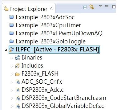
I have a “C2000 2 Phase Interleaved Power Factor Correction Kit” with “Piccolo F28035 Isolated controlCard”. According to the TIDU249 (ILPFC, http://www.ti.com/lit/ug/tidu249/tidu249.pdf), I want to compiler the project (C:\ti\controlSUITE\development_kits\ILPFC_v1.3) to a ram mode for debugging. So,

1. how can I change from F2803x_FLASH mode to F2803x_RAM mode ?

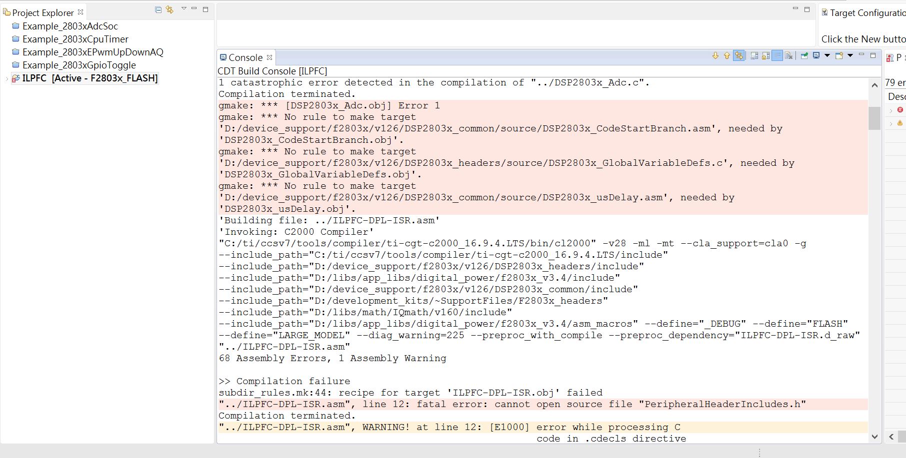
2. There is an error while I going to debug mode. How can I resolve the problem ? 

3. My development environment is Win7 and CCS7.

Any one help will be very appreciated.

Hung-Jin Chen

  • Hung-Jin,

    For the Flash to RAM question:

    Right click on the project name in the explorer window you have shown above.  About 3/4 of the way down the new dialog box you should see a selection called "Build Configurations" hover over this and then pick "Set Active" and you should see an option for RAM build.  After picking this, rebuild the project, and the entire program should load to SRAM.

    For the debugging question, I recommend launching the debug session manually vs via the CCS "Debug" button. To do this:

    1)Right click on your target ccxml in the Target Configurations window.  Select "Launch Target Configuration"

    2)This should open the debug perspective, if not please let me know.  Otherwise, you should observe the C28x CPU listed under the emulation connection.  RIght click on this and select "Connect Target"

    3)At this point if you are connected you can attempt to load code from your project(either RAM or flash)

    Let me know if any of the above steps fail and we can debug more.

    Best,

    Matthew

  • Dear Matthew,

    Q1: I still can not select the RAM mode according your instructuion. Because there is no RAM to select.

    Q2 : there is same error message as above post  while I entry the debug mode. 

    Q3: Could it need a higher version of CCS ? 

    Thank you very much for your help

    Hung-Jin Chen

  • Hung-Jin,

    I looked at this example specifcally and it looks like it was not created with a RAM only build option.  I haven't looked at the code size, but you could see if you can re-direct the flash sections into RAM, but if it is larger than the RAM on the chip this obviously won't work.

    For the connection issue I assume you are using the on-board JTAG chip, via the USB connection.  Note that since this is an isolated config only the JTAG circuit is being powered from that USB connection.  You will still need to supply power to the MCU/main board from the docking station/DIMM connection.  Can you confirm both sides of the iso boundary are powered?

    Best,

    Matthew

  • Dear Matthew,
    1. “C2000 2 Phase Interleaved Power Factor Correction Kit” only has a DIMM socket for “Piccolo F28035 Isolated controlCard” .

    2. “Piccolo F28035 Isolated controlCard” only has a type A USB Port, no  on-board JTAG port.

    3. So, I just can only connect to “Piccolo F28035 Isolated controlCard” by type A USB Port,

    Best regard

    Hung-Jin Chen

  • Hugh-Jin,

    Let me clarify a bit:

    1)2Ph IL PFC Board will need 12V connection at barrel jack, which will give 5V/3.3V output; 5V will get routed through the DIMM to the control CARD to U4 5V->3.3V to power the F28035 MCU

    2)Piccolo F28035 Iso Control Card should have USB Type B mini port labeled J1.  This is routed to a FTDI FT2232D USB to serial CPLD, that is programmed to function as a XDS100v1 debug probe.  However, due to the isolation the 5V from the USB connection does not cross to supply the U4 from above with power.

    So, I want to make sure that both the JTAG debug probe and the MCU have power.

    Best,

    Matthew

  • Dear Matthew,

    1). My Piccolo F28035 Iso Control Card whole name is "CC2803X ISO DIMM REV 1.3". The FTDI  FT2232D USB to serial CPLD is labeled name U9 not U4 and there are 2 green wire to connect  on the PCB's each side to fix some missing wires.

    2).The green LED named LD1 on M6 area  will be turned on while I supply 12V on connection at barrel jack. 

    2). Could you remote control to manipulate this EVM  from USA through TeamViewer utility ?

    if you could, Let's make another appointment some orther day ?

    Best,

    Hung-Jin Chen

  • Hung-Jin,

    I've attached the InfoSheet, which has some quick start info; let's check this to make sure your setup is the same as mine:

    Specifically let's look at page 2, 

    1)When you plug in the USB Type B Mini to the control CARD you should see LED LD4 light up; this indicates that the FTDI/XDS100v1 debug probe has power

    2)When you plug in the 12V to the barrel jack on the bottom board (2Ph IL PFC) and the switch in in the correct posistion you should see LED LD1 light up

    3)Make sure Switch SW3 on the control CARD is "ON" as this enables the TRSTn path to the device

    4)Make sure that the device is in "Wait" Boot mode by putting SW2 as SW2:1 = off and SW2:2 = on.

    Please confirm the above is done and the device still can't connect with CCS.

    Best,

    MatthewF28035_ISOcontrolCARD_InfoSheet.pdf

  • Dear Matthew,

    My EVM already can entry into debug window  after I set the SW2 and SW3 on control CARD as your mention last post.

    Thanks!

    Best,

    Hung-Jin

  • Dear Matthew,

    After your careful guidance, I already can enter the debugging mode of the project. Thank you very much for your help.

    Next, I will trace this project line by line, and look forward to your guidance. I will benefit again.

    Best,

    Hung-Jin

  • Dear Matthew,

    According to the project of C:\ti\controlSUITE\development_kits\ILPFC_v1.3\IL_PFC_F28035_powerSUITE. Within  “ILPFC-Main.c” File 

    May I ask you the following 3 questions ?

    1)  In Line 103, what does the next line mean ?

       103 SineAnalyzer sine_mainsV = SineAnalyzer_DEFAULTS;

    2)  In Line 370 to 372, why say 20KHz interrupt, but line 372 just only write mSec1 * 0.1 = 0.1 mSec = 10 KHz ?

       370 // Configure CPU Timer interrupt for 20KHz interrupt

       371 EALLOW;

       372 CpuTimer2Regs.PRD.all = mSec1 * 0.1;

    3)  May I know what is meaning about “Pin calibration” in line 434 ?

    434 //*********************Pin calibration parameters***********


    Best,

    Hung-Jin Chen

  • A1)The Sine Analyzer function is documented in the User Guide here  C:\ti\controlSUITE\development_kits\ILPFC_v1.3\~Docs/UserGuide-ILPFC-PowerSUITE.pdf page 7: 

    SineAnalyzer.h – this file contains code for calculating the RMS voltage, RMS input current, RMS input power and frequency of the input line voltage. This file has an initialization section (one time execute) and a run-time section which executes at 10kHz rate.


    A2)From what I can see you are correct, the timer is configured for 10kHz vs what the comment says

    A3)I think this is just setting the calcs for the GUI Pin variable.  According to the comments this is from a Chroma supply.

    Best,

    Matthew

  • Dear Matthew

    1). All the following questions are based on the file C: \ ti \ controlSUITE \ development_kits \ ILPFC_v1.0 \ ILPFC-Main.c.

    2). To comment the program, I copied the entire ILFFC_v1.0 project directory, renamed it to ILFFC directory, put it under D: \ ILPFC directory, then rebuilt, but the following error occurred, how can I correct those errors?

    3). According to Figure 4 on page 4 of the tidu249.PDF ( http://www.ti.com/lit/ug/tidu249/tidu249.pdf), could you please tell me where can I find the "10KHz C language interrupt service routine" and "100KHz assembly language interrupt service routine". Please specify the line number and name of program.

    4). The number 10000.0 in lines 548 and 0.1 in line 549, what are meaning?

    548    sine_mainsV.SampleFreq=_IQ15(10000.0);

    549  sine_mainsV.Threshold=_IQ15(0.1);//(0.015);//(0.02);

    5). In the comment on line 563, why is 8 times oversampling required? And, on line 565, why it need Dummy reading?

    6). In lines 580 to 593, the trigger sequence of TrigSel [0] to TrigSel [11] is as follows: EPWM3 → EPWM3 → EPWM4 → EPWM3 → EPWM4 → EPWM1 ​​→ EPWM2 → EPWM1 ​​→ EPWM2 → EPWM1 ​​→ EPWM1 ​​→ EPWM3, What does it mean?

    7). On line 660, I can't find the program DPL_Init (); ,Or how can I use the CCS7's command to find the program?

    Best Regard

    Hung-Jin Chen

  • Hung-Jin,

    Answers inline:

    A2) As long as the new dir is at the same level as the old project this should be OK.  The project is using a relative reference to get to the support files that are in controlSUITE/device_support/  An alternative is that you can manually add the files to the project and that will set the path.

    3). According to Figure 4 on page 4 of the tidu249.PDF ( http://www.ti.com/lit/ug/tidu249/tidu249.pdf), could you please tell me where can I find the "10KHz C language interrupt service routine" and "100KHz assembly language interrupt service routine". Please specify the line number and name of program.

    A3) I beleive that the ASM based ISR is ILPFC-DPL-ISR.asm which is in the project dir.   The C based is in the ILPFC-Main.c file line 1232

    // Digital Power ISR
    interrupt void ILPFC_ISR_wFRA()
    {
    	GpioDataRegs.GPATOGGLE.bit.GPIO2 = 1;
    	#if INCR_BUILD == 1
    		DutyA = SFRA_IQ_INJECT(DutyA_DC);		//Duty1ASetSlewed - Slewed Duty command (Duty1A_Set - set buy user)
    	#elif INCR_BUILD == 2
    		#if BUILD2_SELECT == 0
    			Icmd = SFRA_IQ_INJECT(Icmd_DC);
    		#elif BUILD2_SELECT == 1
    			PFCIcmd_wInj = SFRA_IQ_INJECT(PFCIcmd);
    		#endif
    	#elif INCR_BUILD == 3
    		#if SFRA_TYPE == 0
    			VloopCtr2++;
    			if (VloopCtr2 == VOLTAGE_LOOP_RUN_RATIO)
    			{
    				VbusTargetSlewed_wINJ = SFRA_IQ_INJECT(VbusTargetSlewed);
    				PFCIcmd_wInj = PFCIcmd;
    				VloopCtr2 = 0;
    			}
    		#else
    			PFCIcmd_wInj = SFRA_IQ_INJECT(PFCIcmd);
    			VbusTargetSlewed_wINJ = VbusTargetSlewed;
    		#endif
    	#endif
    
    	DPL_Func();
    
    	#if INCR_BUILD != 3
    		SFRA_IQ_COLLECT(&DutyA,&Ipfc_fltr);
    	#else
    		#if SFRA_TYPE == 0
    			SFRA_IQ_COLLECT(&VbusVcmd, &Vbus);
    		#else
    			SFRA_IQ_COLLECT(&DutyA,&Ipfc_fltr);
    		#endif
    	#endif


    }

    4). The number 10000.0 in lines 548 and 0.1 in line 549, what are meaning?

    548    sine_mainsV.SampleFreq=_IQ15(10000.0);

    549  sine_mainsV.Threshold=_IQ15(0.1);//(0.015);//(0.02);

    A4) I beleive this is setting the sample rate to 10kHz and the voltage threshold to 0.1V.  The _IQ15() function is being use to convert a floating point number to Q15 format since there is not native floating point support on the F28035

    5). In the comment on line 563, why is 8 times oversampling required? And, on line 565, why it need Dummy reading?

    A5) The dummy read is related to an errata on the F28035( http://www.ti.com/lit/sprz295)that the first sample of an ADC conversion sequence is not usuable.  I assume the oversampling in this case is to reduce the noise componet of the sampled signal

    6). In lines 580 to 593, the trigger sequence of TrigSel [0] to TrigSel [11] is as follows: EPWM3 → EPWM3 → EPWM4 → EPWM3 → EPWM4 → EPWM1 ​​→ EPWM2 → EPWM1 ​​→ EPWM2 → EPWM1 ​​→ EPWM1 ​​→ EPWM3, What does it mean?

    A6) This is setting the trigger to convert that respective SOC to the PWMx SOCA/B signal.  From the code it appears that muliple PWMs can triggert the IpfcA input to be sampled

    7). On line 660, I can't find the program DPL_Init (); ,Or how can I use the CCS7's command to find the program?

    A7)THis is in DPlib.h.  If you right click on the DPL_Init() function and then select "open declaration" CCS should open the file in a new tab,

    Best,

    Matt

  • Dear Matt
    Thanks to your help, I have learned a lot from you. Please continue to guide the following questions: Please refer to the ILFFC_main.c file for the following questions 1 to 3.

    1)  On lines 357 to 359, where are the initialization routines for Timer0 to Timer2 ? (It just setting the periods only.)

    2)  On lines 680,

    680 PWMDRV_2ch_UpDwnCnt_Duty1 = &DutyA;

    Although it is part of DPLib, I cannot find a link between DutyA (line 231) and PWMDRV_2ch_UpDwnCnt_Duty1 (line 198). That is, in which program line is DutyA written, and in which program is PWMDRV_2ch_UpDwnCnt_Duty1 referenced?

    (I had already read the DPLib.PDF and Fig.5 of TIDU249.PDF, but I still could not trace the program’s sequence.)

    3)  On lines 680, What does 0.00025 mean?

    685 MATH_EMAVG_Multiplier2=_IQ30(0.00025);


     Please refer to the DSP2803x_ADC.c file for the following questions 4 to 6:

    4)  On lines77 to 82, It should be planned as the analog input of Vfb, but bit.AIO2 = 2, which means disable; may I ask, in which line of the program will it be enabled?

    77 GpioCtrlRegs.AIOMUX1.bit.AIO2 = 2;

    5)  Continue to the previous question, I cannot find a program that ADCINB0 pin is configured as VN_fb.

    6)  On line 211, there is a trigger of SOC0-7, but, why is there no trigger of SOC8-15 before line 228 ?

    211 AdcRegs.ADCSOCFRC1.all = 0x00FF;


    Best Regard

    Hung-Jin, Chen

  • Hung-Jin,

    I'm working on this reply, I expect to post the answer by Wednesday 1/22 US time.  Appreciate your patience.

    Best,

    Matthew

  • Answers below


    1) On lines 357 to 359, where are the initialization routines for Timer0 to Timer2 ? (It just setting the periods only.)

    A1)I believe these are used in the SFRA (Freq analysis) lib, and the init is handled there. These are diagnostic tools, so they may not be leveraged in each project or each project build.

    2) On lines 680,

    680 PWMDRV_2ch_UpDwnCnt_Duty1 = &DutyA;

    Although it is part of DPLib, I cannot find a link between DutyA (line 231) and PWMDRV_2ch_UpDwnCnt_Duty1 (line 198). That is, in which program line is DutyA written, and in which program is PWMDRV_2ch_UpDwnCnt_Duty1 referenced?

    (I had already read the DPLib.PDF and Fig.5 of TIDU249.PDF, but I still could not trace the program’s sequence.)

    A2)These are assembly macros, this particular one is in PWMDRV_2ch_UpDwnCnt.asm which you should see in the main project

    3) On lines 680, What does 0.00025 mean?

    685 MATH_EMAVG_Multiplier2=_IQ30(0.00025);
    A3)The comments are not here, but I beleive that this is setting the # of points of the moving average filter in this case 250 points

    Please refer to the DSP2803x_ADC.c file for the following questions 4 to 6:

    4) On lines77 to 82, It should be planned as the analog input of Vfb, but bit.AIO2 = 2, which means disable; may I ask, in which line of the program will it be enabled?

    77 GpioCtrlRegs.AIOMUX1.bit.AIO2 = 2;

    A4)In this case I beleive that all analog inputs will be used as ADC only, and not the digital type function. So in this case it will remain an ADC input always.

    5) Continue to the previous question, I cannot find a program that ADCINB0 pin is configured as VN_fb.

    A5) This is in the ILPFC-Main.c, do a "find" for for ChSel[11] and you'll see it there

    6) On line 211, there is a trigger of SOC0-7, but, why is there no trigger of SOC8-15 before line 228 ?

    211 AdcRegs.ADCSOCFRC1.all = 0x00FF;


    A6)This is because the trigger for SOC8-15 is set as the INT1 (which is based off EOC7), so as SOC0-7 completes it will trigger SOC8-15 to start. Conversely the trigger for SOC0-7 is set as INT2, which will happen when EOC15 happens. The reason you see a SOCFRC of just SOC0-7 is to start the chain, the while loop will take care of stopping this when the counter size is reached.

  • Dear Matthew,

    Appreciation your reply, concerns about the last response, I still have a confusion about Q1,

    1)     On lines 357 to 359, where are the initialization routines for Timer0 to Timer2 ? (It just setting the periods only.)

    Answer back: I can’t find the Timer initialized Lib in SFRA (Freq analysis) lib.

    Here are the new questions refer to the ILFFC_main.c file for the following questions 

    2)      On lines 680, The DPLib.PDF document cannot find PWMDRV_2ch_UpDwnCnt, but only have PWMDRV_1ch_UpDwnCnt Macro.

    680 PWMDRV_2ch_UpDwnCnt_Duty1 = &DutyA;

    3)      On lines 702, the _IQ24 format of 0.1 is 1677721.6, I cannot realize the Duty is 1677721 meaning ? That’s Duty is represented by percentages (%), isn’t it?

    702 DutyA =_IQ24(0.1); _IQ24(0.1)=1677721.6 ?

    4)      On lines 787and 907, According to TIDU249.pdf file, The A1, equation 4 on page 20, should be -1.

    787 CNTL_2P2Z_CoefStruct1.a1   =_IQ26(1.0);   // A1 = 1

    907 CNTL_2P2Z_CoefStruct2.a1   =_IQ26(1.0); // A1 = 1

    5)      From line 917 to 963, It is explained that when VBUS = OVP = 430V occurs, TZ1 will be touched; but because this circuit is compared using software (on line 954 EPwm2Regs;), and after interrupt is generated through INT3.2, then jump to DPL_ISR service routine, to set both PWM1A and PWM1B to 0, right?

    6)      If Q5 is correct, so when CMPB = 80 is 430V, how is it calculated?

    -----------------------------------------------

    The following question please refer to Interleaved PFC-Settings.h

    7)      On lines 58, What does this line mean?

    58 #define VIN_FULL_RANGE (405.2)//(409.8) //full range of ADC for Vin (each of line and neutral sense)

    8)      On lines 58, the output of ADC is 3.3V while VBUS = 533V, isn’t it?

    60 #define VBUS_FULL_RANGE     (533.00)//(530.45)//(519.0)//full range of ADC for VBUS,if VBUS=533V, then ADC’s output is 3.3V ?

    9)      On lines 61, is the desired output voltage of VBUS ?

    61 #define VBUS_RATED_VOLTS     (390.0) // VBUS desired output ?

    10)  On lines 62, The minimum voltage of VBUS when there is AC input and PFC is off

    62 #define VBUS_MIN ((int32)((160.0/VBUS_FULL_RANGE)*4095*4095)) //Min bus volt with AC in and PFC off

    11)  On lines 64, OVP = 435V ?

    64 #define VBUS_OVP_THRSHLD ((int32)((435.0/VBUS_FULL_RANGE)*4095*4095))

    12)  On lines 66, VBUS_TARGET should be 395V, isn’t it?

    66 #define VBUS_TARGET          ((int32)((VBUS_RATED_VOLTS/VBUS_FULL_RANGE)*4095*4095)) //390V

    13)  On lines 67, I do not realize the meaning about this line and what is NL Vloop ?

    67 #define VBUS_ERROR_NL_CNTRL_THRSHLD ((int32)((15.0/VBUS_FULL_RANGE)*4095*4095)) //Vbus error threshold to activate NL Vloop control.

    14)  On lines 67, Isn't IGain 10.0?

    71 #define I_GAIN      _IQ15(0.995) // (The CS OPAMP Gain = 10.0, not 0.995)?

    15)  On lines 72, What does this line mean? (I know Imax = 19.8A and CS OPAMP Gain = 10.0)

    72 #define R_SHUNT     _IQ15((19.8*0.05/3.0)/(10.0*VIN_FULL_RANGE))

    Best Regard

    Hung-Jin, Chen

  • Hung-Jin,

    I'll need some more time to look into this in detail.  I will try and have a response by the end of the week.

    Best,

    Matthew

  • Hung-Jin,

    My apologies for the delay in getting back to you.  Unfortunately, we'll need a little more time to get answers to your latest questions.  I expect you should hear back from us by mid-next week.

    Regards,

    Joe

  • Dear Matthew

    According to ILPFC-Main.C, the soft start is set by C1 to enter the initial state, and the soft start process is completed by C2, and the elapsed time is controlled by the period of Timer2.

    The line 359 is set the period of Timer2 to 10mSec; the 1307th line is the PFC start-up phase and line 1403 l is the PFC soft-start mode.

    359 CpuTimer2Regs.PRD.all = mSec10;

    1370 void C1(void) // PFC Start Phase

    1403 void C2(void) //PFC Soft Start Mode

    According to the analysis of C1 and C2 state machine, the time to complete the C2 state machine should be about 2.8 seconds; I used an oscilloscope to grab the soft start of the EVM board but it was 8.5 seconds; that is, the period of Timer2 is not 10mSec, but 16.7Hz.

    Why is this happening?

    Hung-Jin Chen