Part Number: TMS320F28335
Tool/software: Code Composer Studio
Dear Sir/Madam,
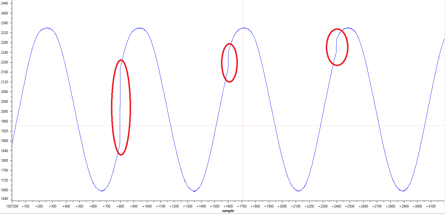
I am using TMSDOCKF28335 hardware with control card. I am giving sine signal from outside with 50Hz through signal conditioner shifted by 1.5V and range is between 0 to 3V. Here I am collecting samples through epwm trigger. Epwm1 is running with the frequency of 40kHz according to that I have to get 800 samples to construct complete sine signal. I am able to log 800 samples but there is one glitch is repeating for every 800 sample I need pure sine waveform. But I am unable get the desired signal. Because of this problem my SPLL is getting worse for every few cycles of sine wave. Here I am attaching the code I used and also Linker command file along with the waveforms.Please suggest something.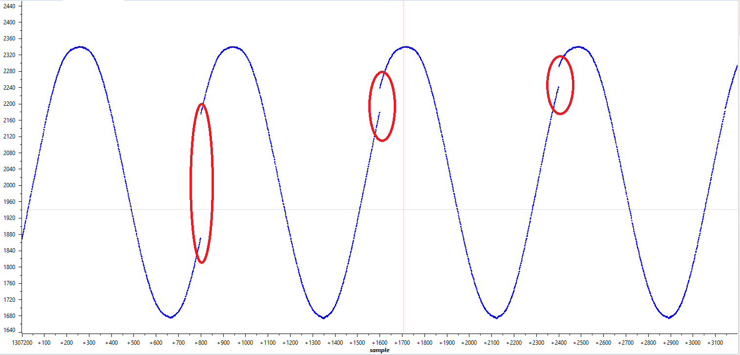
//###########################################################################
//
// FILE:   Example_2833xAdcSoc.c
//
// TITLE:  ADC Start of Conversion Example
//
//! \addtogroup f2833x_example_list
//! <h1> ADC Start of Conversion (adc_soc)</h1>
//!
//! This ADC example uses ePWM1 to generate a periodic ADC SOC on SEQ1.
//! Two channels are converted, ADCINA3 and ADCINA2.
//!
//! \b Watch \b Variables \n
//! - Voltage1[10]	- Last 10 ADCRESULT0 values
//! - Voltage2[10]	- Last 10 ADCRESULT1 values
//! - ConversionCount	- Current result number 0-9
//! - LoopCount		- Idle loop counter
//
//###########################################################################
// $TI Release: F2833x Support Library v2.00.00.00 $
// $Release Date: Sun Sep 29 07:33:44 CDT 2019 $
// $Copyright:
// Copyright (C) 2009-2019 Texas Instruments Incorporated - http://www.ti.com/
//
// Redistribution and use in source and binary forms, with or without
// modification, are permitted provided that the following conditions
// are met:
//
//   Redistributions of source code must retain the above copyright
//   notice, this list of conditions and the following disclaimer.
//
//   Redistributions in binary form must reproduce the above copyright
//   notice, this list of conditions and the following disclaimer in the
//   documentation and/or other materials provided with the
//   distribution.
//
//   Neither the name of Texas Instruments Incorporated nor the names of
//   its contributors may be used to endorse or promote products derived
//   from this software without specific prior written permission.
//
// THIS SOFTWARE IS PROVIDED BY THE COPYRIGHT HOLDERS AND CONTRIBUTORS
// "AS IS" AND ANY EXPRESS OR IMPLIED WARRANTIES, INCLUDING, BUT NOT
// LIMITED TO, THE IMPLIED WARRANTIES OF MERCHANTABILITY AND FITNESS FOR
// A PARTICULAR PURPOSE ARE DISCLAIMED. IN NO EVENT SHALL THE COPYRIGHT
// OWNER OR CONTRIBUTORS BE LIABLE FOR ANY DIRECT, INDIRECT, INCIDENTAL,
// SPECIAL, EXEMPLARY, OR CONSEQUENTIAL DAMAGES (INCLUDING, BUT NOT
// LIMITED TO, PROCUREMENT OF SUBSTITUTE GOODS OR SERVICES; LOSS OF USE,
// DATA, OR PROFITS; OR BUSINESS INTERRUPTION) HOWEVER CAUSED AND ON ANY
// THEORY OF LIABILITY, WHETHER IN CONTRACT, STRICT LIABILITY, OR TORT
// (INCLUDING NEGLIGENCE OR OTHERWISE) ARISING IN ANY WAY OUT OF THE USE
// OF THIS SOFTWARE, EVEN IF ADVISED OF THE POSSIBILITY OF SUCH DAMAGE.
// $
//###########################################################################

//
// Included Files
//
#include "DSP28x_Project.h"     // Device Headerfile and Examples Include File

//
// Function Prototypes
//
__interrupt void adc_isr(void);

//
// Globals
//
Uint16 LoopCount;
Uint16 ConversionCount;
Uint16 VG[800];


//
// Main
//
void main(void)
{
    //
    // Step 1. Initialize System Control:
    // PLL, WatchDog, enable Peripheral Clocks
    // This example function is found in the DSP2833x_SysCtrl.c file.
    //
    InitSysCtrl();

    EALLOW;
    #if (CPU_FRQ_150MHZ)     // Default - 150 MHz SYSCLKOUT
        //
        // HSPCLK = SYSCLKOUT/2*ADC_MODCLK2 = 150/(2*3)   = 25.0 MHz
        //
        #define ADC_MODCLK 0x3
    #endif
    #if (CPU_FRQ_100MHZ)
        //
        // HSPCLK = SYSCLKOUT/2*ADC_MODCLK2 = 100/(2*2)   = 25.0 MHz
        //
        #define ADC_MODCLK 0x2
    #endif
    EDIS;

    //
    // Define ADCCLK clock frequency ( less than or equal to 25 MHz )
    // Assuming InitSysCtrl() has set SYSCLKOUT to 150 MHz
    //
    EALLOW;
    SysCtrlRegs.HISPCP.all = ADC_MODCLK;
    EDIS;

    //
    // Step 2. Initialize GPIO:
    // This example function is found in the DSP2833x_Gpio.c file and
    // illustrates how to set the GPIO to it's default state.
    //
    // InitGpio();  // Skipped for this example

    //
    // Step 3. Clear all interrupts and initialize PIE vector table:
    // Disable CPU interrupts
    //
    DINT;

    //
    // Initialize the PIE control registers to their default state.
    // The default state is all PIE interrupts disabled and flags
    // are cleared.
    // This function is found in the DSP2833x_PieCtrl.c file.
    //
    InitPieCtrl();

    //
    // Disable CPU interrupts and clear all CPU interrupt flags:
    //
    IER = 0x0000;
    IFR = 0x0000;

    //
    // Initialize the PIE vector table with pointers to the shell Interrupt
    // Service Routines (ISR).
    // This will populate the entire table, even if the interrupt
    // is not used in this example.  This is useful for debug purposes.
    // The shell ISR routines are found in DSP2833x_DefaultIsr.c.
    // This function is found in DSP2833x_PieVect.c.
    //
    InitPieVectTable();

    //
    // Interrupts that are used in this example are re-mapped to
    // ISR functions found within this file.
    //
    EALLOW;  // This is needed to write to EALLOW protected register
    PieVectTable.ADCINT = &adc_isr;
    EDIS;    // This is needed to disable write to EALLOW protected registers

    //
    // Step 4. Initialize all the Device Peripherals:
    // This function is found in DSP2833x_InitPeripherals.c
    //
    // InitPeripherals(); // Not required for this example
    InitAdc();  // For this example, init the ADC

    //
    // Step 5. User specific code, enable interrupts:
    //

    //
    // Enable ADCINT in PIE
    //
    PieCtrlRegs.PIEIER1.bit.INTx6 = 1;
    IER |= M_INT1;      // Enable CPU Interrupt 1
    EINT;               // Enable Global interrupt INTM
    ERTM;               // Enable Global realtime interrupt DBGM

    LoopCount = 0;
    ConversionCount = 0;

    //
    // Configure ADC
    //
    AdcRegs.ADCMAXCONV.all = 0x0000;       // Setup 2 conv's on SEQ1
    AdcRegs.ADCCHSELSEQ1.bit.CONV00 = 0x2; // Setup ADCINA3 as 1st SEQ1 conv.

    //
    // Enable SOCA from ePWM to start SEQ1
    //
    AdcRegs.ADCTRL2.bit.EPWM_SOCA_SEQ1 = 1;

    AdcRegs.ADCTRL2.bit.INT_ENA_SEQ1 = 1;  // Enable SEQ1 interrupt (every EOS)

    //
    // Assumes ePWM1 clock is already enabled in InitSysCtrl();
    //
    EPwm1Regs.ETSEL.bit.SOCAEN = 1;     // Enable SOC on A group
    EPwm1Regs.ETSEL.bit.SOCASEL = 4;    // Select SOC from from CPMA on upcount
    EPwm1Regs.ETPS.bit.SOCAPRD = 1;     // Generate pulse on 1st event
    EPwm1Regs.CMPA.half.CMPA = 1875;	// Set compare A value
    EPwm1Regs.TBPRD = 3750;           // Set period for ePWM1
    EPwm1Regs.TBCTL.bit.CTRMODE = 0;	// count up and start
    EPwm1Regs.TBCTL.bit.HSPCLKDIV=0;
    EPwm1Regs.TBCTL.bit.CLKDIV=0;

    //
    // Wait for ADC interrupt
    //
    for(;;)
    {
        LoopCount++;
    }
}

//
// adc_isr -
//
__interrupt void
adc_isr(void)
{
    VG[ConversionCount] = AdcRegs.ADCRESULT0 >>4;


    //
    // If 40 conversions have been logged, start over
    //
    if(ConversionCount == 800)
    {
        ConversionCount = 0;
    }
    else
    {
        ConversionCount++;
    }

    //
    // Reinitialize for next ADC sequence
    //
    AdcRegs.ADCTRL2.bit.RST_SEQ1 = 1;         // Reset SEQ1
    AdcRegs.ADCST.bit.INT_SEQ1_CLR = 1;       // Clear INT SEQ1 bit
    PieCtrlRegs.PIEACK.all = PIEACK_GROUP1;   // Acknowledge interrupt to PIE

    return;
}

//
// End of File
//
/*
// TI File $Revision: /main/11 $
// Checkin $Date: April 15, 2009   09:57:28 $
//###########################################################################
//
// FILE:    28335_RAM_lnk.cmd
//
// TITLE:   Linker Command File For 28335 examples that run out of RAM
//
//          This ONLY includes all SARAM blocks on the 28335 device.
//          This does not include flash or OTP.
//
//          Keep in mind that L0 and L1 are protected by the code
//          security module.
//
//          What this means is in most cases you will want to move to
//          another memory map file which has more memory defined.
//
//###########################################################################
// $TI Release: F2833x Support Library v2.00.00.00 $
// $Release Date: Sun Sep 29 07:33:44 CDT 2019 $
// $Copyright:
// Copyright (C) 2009-2019 Texas Instruments Incorporated - http://www.ti.com/
//
// Redistribution and use in source and binary forms, with or without
// modification, are permitted provided that the following conditions
// are met:
//
//   Redistributions of source code must retain the above copyright
//   notice, this list of conditions and the following disclaimer.
//
//   Redistributions in binary form must reproduce the above copyright
//   notice, this list of conditions and the following disclaimer in the
//   documentation and/or other materials provided with the
//   distribution.
//
//   Neither the name of Texas Instruments Incorporated nor the names of
//   its contributors may be used to endorse or promote products derived
//   from this software without specific prior written permission.
//
// THIS SOFTWARE IS PROVIDED BY THE COPYRIGHT HOLDERS AND CONTRIBUTORS
// "AS IS" AND ANY EXPRESS OR IMPLIED WARRANTIES, INCLUDING, BUT NOT
// LIMITED TO, THE IMPLIED WARRANTIES OF MERCHANTABILITY AND FITNESS FOR
// A PARTICULAR PURPOSE ARE DISCLAIMED. IN NO EVENT SHALL THE COPYRIGHT
// OWNER OR CONTRIBUTORS BE LIABLE FOR ANY DIRECT, INDIRECT, INCIDENTAL,
// SPECIAL, EXEMPLARY, OR CONSEQUENTIAL DAMAGES (INCLUDING, BUT NOT
// LIMITED TO, PROCUREMENT OF SUBSTITUTE GOODS OR SERVICES; LOSS OF USE,
// DATA, OR PROFITS; OR BUSINESS INTERRUPTION) HOWEVER CAUSED AND ON ANY
// THEORY OF LIABILITY, WHETHER IN CONTRACT, STRICT LIABILITY, OR TORT
// (INCLUDING NEGLIGENCE OR OTHERWISE) ARISING IN ANY WAY OUT OF THE USE
// OF THIS SOFTWARE, EVEN IF ADVISED OF THE POSSIBILITY OF SUCH DAMAGE.
// $
//###########################################################################
*/

/* ======================================================
// For Code Composer Studio V2.2 and later
// ---------------------------------------
// In addition to this memory linker command file,
// add the header linker command file directly to the project.
// The header linker command file is required to link the
// peripheral structures to the proper locations within
// the memory map.
//
// The header linker files are found in <base>\headers\cmd
//
// For BIOS applications add:      DSP2833x_Headers_BIOS.cmd
// For nonBIOS applications add:   DSP2833x_Headers_nonBIOS.cmd
========================================================= */

/* ======================================================
// For Code Composer Studio prior to V2.2
// --------------------------------------
// 1) Use one of the following -l statements to include the
// header linker command file in the project. The header linker
// file is required to link the peripheral structures to the proper
// locations within the memory map                                    */

/* Uncomment this line to include file only for non-BIOS applications */
/* -l DSP2833x_Headers_nonBIOS.cmd */

/* Uncomment this line to include file only for BIOS applications */
/* -l DSP2833x_Headers_BIOS.cmd */

/* 2) In your project add the path to <base>\headers\cmd to the
   library search path under project->build options, linker tab,
   library search path (-i).
/*========================================================= */

/* Define the memory block start/length for the F28335
   PAGE 0 will be used to organize program sections
   PAGE 1 will be used to organize data sections

   Notes:
         Memory blocks on F28335 are uniform (ie same
         physical memory) in both PAGE 0 and PAGE 1.
         That is the same memory region should not be
         defined for both PAGE 0 and PAGE 1.
         Doing so will result in corruption of program
         and/or data.

         L0/L1/L2 and L3 memory blocks are mirrored - that is
         they can be accessed in high memory or low memory.
         For simplicity only one instance is used in this
         linker file.

         Contiguous SARAM memory blocks can be combined
         if required to create a larger memory block.
*/


MEMORY
{
PAGE 0 :
   /* BEGIN is used for the "boot to SARAM" bootloader mode      */

   BEGIN      : origin = 0x000000, length = 0x000002     /* Boot to M0 will go here                      */
   RAMM0      : origin = 0x000050, length = 0x0003B0
   RAML0      : origin = 0x008000, length = 0x001000
   RAML1      : origin = 0x009000, length = 0x001000
   RAML2      : origin = 0x00A000, length = 0x001000
   RAML3      : origin = 0x00B000, length = 0x001000
   ZONE7A     : origin = 0x200000, length = 0x00FC00    /* XINTF zone 7 - program space */
   CSM_RSVD   : origin = 0x33FF80, length = 0x000076     /* Part of FLASHA.  Program with all 0x0000 when CSM is in use. */
   CSM_PWL    : origin = 0x33FFF8, length = 0x000008     /* Part of FLASHA.  CSM password locations in FLASHA            */
   ADC_CAL    : origin = 0x380080, length = 0x000009
   RESET      : origin = 0x3FFFC0, length = 0x000002
   IQTABLES   : origin = 0x3FE000, length = 0x000b50
   IQTABLES2  : origin = 0x3FEB50, length = 0x00008c
   FPUTABLES  : origin = 0x3FEBDC, length = 0x0006A0
   BOOTROM    : origin = 0x3FF27C, length = 0x000D44


PAGE 1 :
   /* BOOT_RSVD is used by the boot ROM for stack.               */
   /* This section is only reserved to keep the BOOT ROM from    */
   /* corrupting this area during the debug process              */

   BOOT_RSVD  : origin = 0x000002, length = 0x00004E     /* Part of M0, BOOT rom will use this for stack */
   RAMM1      : origin = 0x000400, length = 0x000400     /* on-chip RAM block M1 */
   RAML4      : origin = 0x00C000, length = 0x001000
   RAML5      : origin = 0x00D000, length = 0x001000
   RAML6      : origin = 0x00E000, length = 0x001000
   RAML7      : origin = 0x00F000, length = 0x001000
   ZONE7B     : origin = 0x20FC00, length = 0x000400     /* XINTF zone 7 - data space */
}


SECTIONS
{
   /* Setup for "boot to SARAM" mode:
      The codestart section (found in DSP28_CodeStartBranch.asm)
      re-directs execution to the start of user code.  */
   codestart        : > BEGIN,     PAGE = 0
   ramfuncs         : > RAML0,     PAGE = 0
   .text            : >> RAML1 | RAML2,     PAGE = 0
   .InitBoot        : > RAML1,     PAGE = 0
   .cinit           : > RAML0,     PAGE = 0
   .pinit           : > RAML0,     PAGE = 0
   .switch          : > RAML0,     PAGE = 0

   .stack           : > RAMM1,     PAGE = 1
   .ebss            : > RAML4,     PAGE = 1
   .econst          : > RAML5,     PAGE = 1
   .esysmem         : > RAMM1,     PAGE = 1

   IQmath           : > RAML1,     PAGE = 0
   IQmathTables     : > IQTABLES,  PAGE = 0, TYPE = NOLOAD

   /* Uncomment the section below if calling the IQNexp() or IQexp()
      functions from the IQMath.lib library in order to utilize the
      relevant IQ Math table in Boot ROM (This saves space and Boot ROM
      is 1 wait-state). If this section is not uncommented, IQmathTables2
      will be loaded into other memory (SARAM, Flash, etc.) and will take
      up space, but 0 wait-state is possible.
   */
   /*
   IQmathTables2    : > IQTABLES2, PAGE = 0, TYPE = NOLOAD
   {

              IQmath.lib<IQNexpTable.obj> (IQmathTablesRam)

   }
   */

   FPUmathTables    : > FPUTABLES, PAGE = 0, TYPE = NOLOAD

   DMARAML4         : > RAML4,     PAGE = 1
   DMARAML5         : > RAML5,     PAGE = 1
   DMARAML6         : > RAML6,     PAGE = 1
   DMARAML7         : > RAML7,     PAGE = 1

   ZONE7DATA        : > ZONE7B,    PAGE = 1

   .reset           : > RESET,     PAGE = 0, TYPE = DSECT /* not used                    */
   csm_rsvd         : > CSM_RSVD   PAGE = 0, TYPE = DSECT /* not used for SARAM examples */
   csmpasswds       : > CSM_PWL    PAGE = 0, TYPE = DSECT /* not used for SARAM examples */

   /* Allocate ADC_cal function (pre-programmed by factory into TI reserved memory) */
   .adc_cal     : load = ADC_CAL,   PAGE = 0, TYPE = NOLOAD

}

/*
//===========================================================================
// End of file.
//===========================================================================
*/