This thread has been locked.

If you have a related question, please click the "Ask a related question" button in the top right corner. The newly created question will be automatically linked to this question.

TMS320F280049: read data from multiple SPI salvers in one switch cycle

Part Number: TMS320F280049

Dear C2000 expert,

I'm currently using F280049 to design a power module. Due to there is a isolation between MCU and sensed signals, a extern adc with isolator was used, and the adc result will be sent to F280049 through SPI interface. 

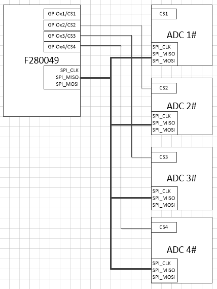
Below picture shows the diagram of F280049 and 4 external adcs. F280049 is SPI master, and the 4 adcs are SPI slavers. And CS signal was controled by different GPIOs in F280049, I'd like to get the all 4 adcs result in one switch cycle, because all those signals are used as feedbacks for control loop, can you please share some suggestions?

I don't want take much CPU usages due to the switch frequency is 200KHZ. The conversion speed of ADC is very fast, the adc was triggered to start conversion by CS signal pull low. 

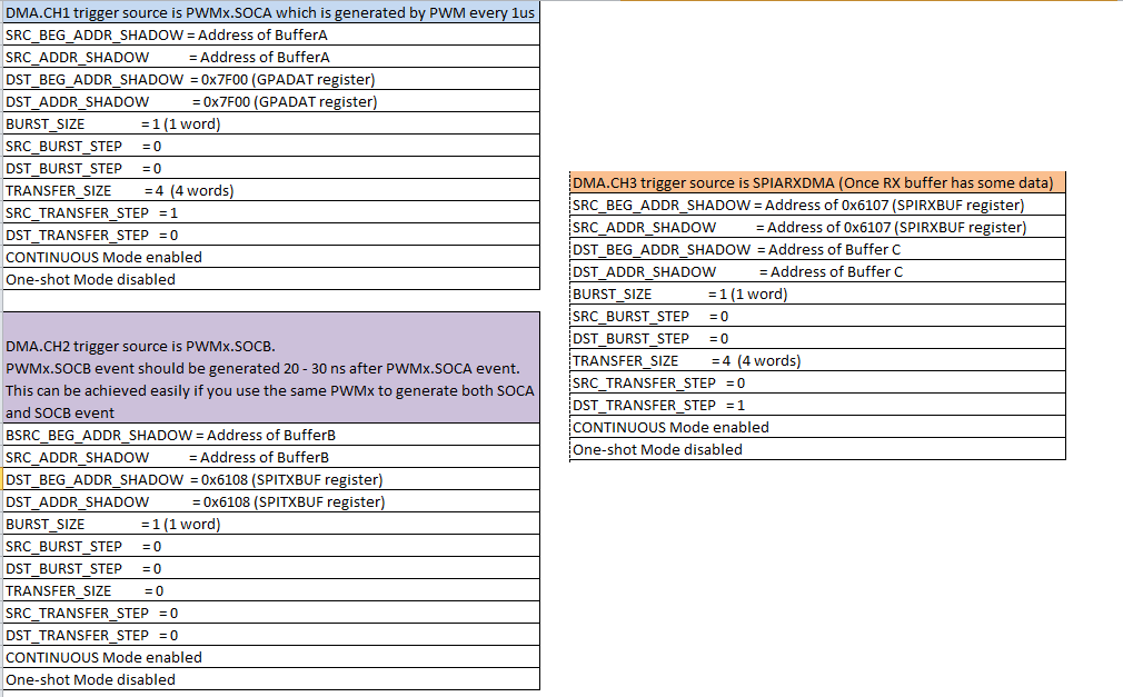
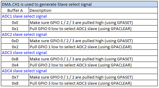
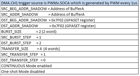
If there are some ways of triggering spi to read external adcs automatically without CPU intervention, that would be perfect. Thanks

  • Jack,

    I'm not clear what you mean by saying "I'd like to get the all 4 adcs result in one switch cycle"? Please elaborate.

    I don't see how you can trigger SPI to receive ADC results register without CPU intervention.

    Regards,

    Manoj

  • Hi Manoj,

    Thanks for your reply, and sorry to bring confusion to you.

    Currenly I didn't have much good idea of this, and trigger the spi in each switch cycle isr, it has to use CPU resources.

    Please see below sample sequence, it has to take 4 switch cycles for reading all signals, and it's not very good for response performance. So I'd like to know if there is a good way for sensing those signals.

    Sampling sequency in my currently configuration

    ... ...

    Switch cycle n - 1 isr: trigger adc 4#, and read adc 3#

    Switch cycle n isr: trigger adc 1#, and read adc 4#

    Switch cycle n + 1 isr: trigger adc 2#, and read adc 1#

    Switch cycle n + 2 isr: trigger adc 3#, and read adc 2#

    Switch cycle n + 3 isr: trigger adc 4#, and read adc 3#

    Switch cycle n + 4 isr: trigger adc 1#, and read adc 4#

    ... ...

    In this case, spi was used in fast speed mode which is 25Mhz,and read single adc takes 16 clocks.

  • Jack,

    Here is my understanding of what you are trying to achieve.

    Goal: You need to read the ADC results of all the 4 ADC slaves every 5us (200 KHz) with minimal (or) no CPU intervention as possible.

    Possible solution: If this is the goal, you can possibly achieve this using 3 DMA channels, 1 PWM (to generate SOCA / SOCB events to trigger DMA Channels 1 and 2). Once all the 4 ADC slave results are available you can generate CPU interrupt. Essentially, this method will ensure you get CPU interrupt only after all the 4 ADC slave results are ready.

    In order to initiate SPI receive from slave, here are the common steps:

    1) Pull SPIASTE low, this requires you to pull down corresponding GPIO low

    2) Wait for specified amount defined parameter "Delay time, SPISTE valid to SPICLK" available in SPI tables in DS

    3) Initiate dummy SPI Transmit. This can be done by writing 0x0000 to SPITXBUF register which is equivalent to using SPI_writeDataNonBlocking driverlib function

    4) Read SPIRXBUF to get the ADC result after SPIRXBUF has receive data. This is equivalent to using SPI_readDataBlocking driverlib function.

    The above step can be achieved by using 3 DMA channels as shown below:

    1. DMA.CH1 needs to be configured to be triggered by PWMx.SOCA event. This DMA.CH1 is used to generate slave select signal.
    2. DMA.CH2 needs to be configured to be triggered by PWMx.SOCB event. This DMA.CH2 is used to do dummy writes of 0x0000 to SPITXBUF.
    3. DMA.CH3 need to be configured to be triggered by SPIRXDMA event. This DMA.CH3 is used to read SPIRXBUF register.

    DMA conceptual configuration details for different channel used is mentioned below:-

    DMA.CH1 ePIE interrupt needs to be disabled

    DMA.CH2 ePIE interrupt needs to be disabled

    DMA.CH3 ePIE interrupt needs to be enabled

    Hopefully this helps!

    Regards,

    Manoj

  • Hi Manoj,

    Thanks for your support here, this is very brilliant idea and it's what I want to achieve. 

    Regarding to slave select signals, if it writes to GPADAT register, then the other GPIOs (except GPIO 0/1/2/3) will be affacted. Is there any way to just modify the expected GPIO in DMA? How about to use GPASET and GPACLEAR register together?

  • Jack,

    Yes, you can use GPASET and GPACLEAR registers to get the same effect. You need to do the following changes to above configuration.

    1. DMA.CH1 needs to be configured to control both GPASET and GPACLEAR on the same DMA trigger
    2. DMA.CH1 configuration needs to be changed to have burst size of 2 and destination address needs to be changed to GPASET register. On a DMA.CH1 trigger from PWMx.SOCA, both GPASET and GPACLEAR get appropriated configured.

    Regards,

    Manoj

  • Hi Manoj,

    Thanks for your great support here. I have implemented code to realize your proposal, currently it works.Thanks again.

  • Hi Manoj,

    One more question about the CH1 configuration, from the DMA state machine, SRC/DST_ADDR_ACTIVE will be increamented by a step in each burst.

    Suppose I have followed your proposal of configuration CH1, then the single transfer will be shown as follow. The destination active address register value from second to forth burst will not what I expected, isn't it? If my understanding is wrong, please help to correct it.

    The first burst(I think this is triggered by EPWMx.SOCA)
    SRC_ADDR_ACTIVE = &BufferA[0]
    DST_ADDR_ACTIVE = 0x7F02; /*GPASET*/

    SRC_ADDR_ACTIVE = &BufferA[1]
    DST_ADDR_ACTIVE = 0x7F04; /*GPACLEAR*/

    The second burst:
    SRC_ADDR_ACTIVE = &BufferA[2]
    DST_ADDR_ACTIVE = 0x7F04; /* GPACLEAR. it will use the last DST_ADDR_ACTIVE value since DST transfer step set to 0 */

    SRC_ADDR_ACTIVE = &BufferA[3]
    DST_ADDR_ACTIVE = 0x7F06; /*GPATOGGLE*/

    The third burst:
    SRC_ADDR_ACTIVE = &BufferA[4]
    DST_ADDR_ACTIVE = 0x7F06; /* GPATOGGLE. it will use the last DST_ADDR_ACTIVE value since DST transfer step set to 0 */

    SRC_ADDR_ACTIVE = &BufferA[5]
    DST_ADDR_ACTIVE = 0x7F08; /* GPBDAT */

    The forth burst:
    SRC_ADDR_ACTIVE = &BufferA[6]
    DST_ADDR_ACTIVE = 0x7F08; /* GPBDAT. it will use the last DST_ADDR_ACTIVE value since DST transfer step set to 0 */

    SRC_ADDR_ACTIVE = &BufferA[7]
    DST_ADDR_ACTIVE = 0x7F0a; /* GPBSET */

  • Hi Manoj,

    Regarding to CH1 of setting both GPASET and GPACLEAR register, how about to use wrap around function?

    If I set both DST_WRAP_SIZE and DSP_WRAP_STEP to 0, then the DST_ADDR_ACTIVE will be wrap around to the beging register(GPASET) in each burst.

    The sequence shown as below:

    The first burst(I think this is triggered by EPWMx.SOCA)
    SRC_ADDR_ACTIVE = &BufferA[0]
    DST_ADDR_ACTIVE = 0x7F02; /*GPASET*/
    ||
    \/
    SRC_ADDR_ACTIVE = &BufferA[1]
    DST_ADDR_ACTIVE = 0x7F04; /*GPACLEAR*/

    The second burst:
    SRC_ADDR_ACTIVE = &BufferA[2]
    DST_ADDR_ACTIVE = 0x7F02; /* GPACLEAR. Wrap arround to the begine of address. Set both wrap size and step to 0 */
    ||
    \/
    SRC_ADDR_ACTIVE = &BufferA[3]
    DST_ADDR_ACTIVE = 0x7F04; /*GPACLEAR*/

    The third burst:
    SRC_ADDR_ACTIVE = &BufferA[4]
    DST_ADDR_ACTIVE = 0x7F02; /* GPACLEAR. Wrap arround to the begine of address. Set both wrap size and step to 0 */
    ||
    \/
    SRC_ADDR_ACTIVE = &BufferA[5]
    DST_ADDR_ACTIVE = 0x7F04; /*GPACLEAR*/

    The forth burst:
    SRC_ADDR_ACTIVE = &BufferA[6]
    DST_ADDR_ACTIVE = 0x7F02; /* GPACLEAR. Wrap arround to the begine of address. Set both wrap size and step to 0 */
    ||
    \/
    SRC_ADDR_ACTIVE = &BufferA[7]
    DST_ADDR_ACTIVE = 0x7F04; /*GPACLEAR*/

  • Jack,

    I believe you have got the code to work using wrap feature. I don't see any question. Can I consider this issue closed?

    Regards,

    Manoj

  • Hi Manoj,

    No, currently the spia tx and rx with using DMA works, but the chip select signals still can't work.  Here is my dma initialization code, can you please help to take a look at it? Thanks...

    #pragma DATA_SECTION(spi_src_sel, "ramgs0"); /* spi select buffer*/
    static Uint32 spi_src_sel[2*NOF_SIGNALS] = {
    ADC1_GPASET,
    ADC1_GPACLEAR,
    ADC2_GPASET,
    ADC2_GPACLEAR,
    ADC3_GPASET,
    ADC3_GPACLEAR,
    ADC4_GPASET,
    ADC4_GPACLEAR,
    };

    /* **** Function Definitions **** */
    void init_spia_dma(void)
    {
    //
    // Initialize DMA
    //
    DMA_initController();

    /* uint32_t base, const void *destAddr, const void *srcAddr */
    DMA_configAddresses(DMA_CH1_BASE, (int32_t *)&GpioDataRegs.GPASET, (uint32_t *)spi_src_sel);
    /* base, size, srcStep, destStep */
    DMA_configBurst( DMA_CH1_BASE, 2, 2, 2);
    DMA_configTransfer(DMA_CH1_BASE, 4, 2, 0);
    /* base, srcWrapSize, srcStep, destWrapSize, destStep */
    DMA_configWrap(DMA_CH1_BASE, 0xFFF0, 0, 1, 0 );

    DMA_configMode(DMA_CH1_BASE, DMA_TRIGGER_EPWM4SOCA, DMA_CFG_ONESHOT_DISABLE |
    DMA_CFG_CONTINUOUS_ENABLE | DMA_CFG_SIZE_32BIT);

    /* uint32_t base, const void *destAddr, const void *srcAddr */
    DMA_configAddresses(DMA_CH2_BASE, (uint32_t *)&SpiaRegs.SPITXBUF, (uint32_t *)ext_dacValue);
    /* base, size, srcStep, destStep */
    DMA_configBurst( DMA_CH2_BASE, 1, 0, 0);
    DMA_configTransfer(DMA_CH2_BASE, 4, 1, 0);

    /* base, srcWrapSize, srcStep, destWrapSize, destStep */
    DMA_configWrap(DMA_CH2_BASE, 0xFFF0, 0, 0xFFF0, 0 );

    DMA_configMode(DMA_CH2_BASE, DMA_TRIGGER_EPWM4SOCB, DMA_CFG_ONESHOT_DISABLE |
    DMA_CFG_CONTINUOUS_ENABLE | DMA_CFG_SIZE_16BIT);

    /* uint32_t base, const void *destAddr, const void *srcAddr */
    DMA_configAddresses(DMA_CH3_BASE, (uint32_t *)ext_adcResult, (uint32_t *)&SpiaRegs.SPIRXBUF);
    /* base, size, srcStep, destStep */
    DMA_configBurst( DMA_CH3_BASE, 1, 0, 0);
    DMA_configTransfer(DMA_CH3_BASE, 4, 0, 1);
    /* base, srcWrapSize, srcStep, destWrapSize, destStep */
    DMA_configWrap(DMA_CH3_BASE, 0xFFF0, 0, 0xFFF0, 0 );

    DMA_configMode(DMA_CH3_BASE, DMA_TRIGGER_SPIARX, DMA_CFG_ONESHOT_DISABLE |
    DMA_CFG_CONTINUOUS_ENABLE | DMA_CFG_SIZE_16BIT);

    DMA_enableTrigger(DMA_CH1_BASE);
    DMA_enableTrigger(DMA_CH2_BASE);
    DMA_enableTrigger(DMA_CH3_BASE);

    DMA_startChannel(DMA_CH1_BASE);
    DMA_startChannel(DMA_CH2_BASE);
    DMA_startChannel(DMA_CH3_BASE);

    init_dma_trigger_cfg();
    }

  • Hi Manoj,

    One more question, I didn't see the datasheet mentioned that GPIO register could be accessed by DMA, can you please help to double confirm it?

  • This may not be resolved, since the chip select signal still can not be generated by DMA to configure GPASET & GPALEAR.

  • Jack,

    Yes, you're right!

    DMA doesn't have access to GPIO DATA registers on this device.

    So, you have to use CPU interrupt (or) CLA task to drive corresponding GPIO pins low to enable slave select.

    This changes the implmentation as shown below:-

    1) Use PWMx.SOCA to trigger CPU interrupt (or) CLA task to configure slave select signal

    2) DMA.CH2 configurations can be the same as what we discussed above

    3) DMA.CH3 configurations can be the same as what we discussed above

    Regards,

    Manoj