Part Number: LAUNCHXL-F28379D
Tool/software: Code Composer Studio
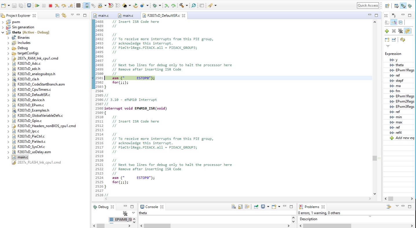
I intend to run a three phase system ( three inverter per phase), The written code below builds, debugs and runs only when PWM9 has not been programmed. However, when I program the PWM9 port, the program build and debug successfully but doesn't run. instead the attached page (F2837xD_DefaultISR.c) pop up and the system doesn't work. I really don't know hoe to resolve the problem. The same paper appears when I configure PWm10, PWM11, PWM12...
Do I need to add a specific file to my project?
// Included Files
// I wish to run a three phase system, three inverter per phase
#include "F28x_Project.h"
#include <stdlib.h>
#define TIMER_TBPRD 12500 // Period register
#define EXAMPLE1 1 // Basic pinout configuration example
#define EXAMPLE2 0 // Communication pinout example
#define start1 GpioDataRegs.GPBDAT.bit.GPIO62// button PB1 just blink 58-61
#define stop1 GpioDataRegs.GPBDAT.bit.GPIO63 // button PB1
#define start GpioDataRegs.GPCDAT.bit.GPIO68// button PB1 just blink 58-61
#define stop GpioDataRegs.GPCDAT.bit.GPIO69 // button PB1
#define DELAY 0
double fm= 0; double PB1= 0; double PB2=0; double PB3= 0; double PB4=0;
double y00= 0; double y11=0; double y22= 0;
double fc= 4000; double max1= 0; double max=0; double min1= 0; double min=0;
double theta=0;
double y2=0; double yr2=0; double y90=0; double vd=0;
double y1=0; double yr1=0;
double y=0; double yr=0;
double refr=0;
double refr1=0; double ref1=0; double ref2=0; double ref=0; double refd=0; double refd1=0; double refd2=0;
double refr2=0;
double ma=0;
double stepma = 0;
double stepf = 0;
double vf = 0.01667;
// Function Prototypes
#define EXAMPLE1 1
void Gpio_setup1(void);
void InitEPwm1Example(void);
void InitEPwm2Example(void);
void InitEPwm3Example(void);
void InitEPwm4Example(void);
void InitEPwm5Example(void);
void InitEPwm6Example(void);
void InitEPwm7Example(void);
void InitEPwm8Example(void);
void InitEPwm9Example(void);
__interrupt void epwm1_isr(void);
__interrupt void epwm2_isr(void);
__interrupt void epwm3_isr(void);
__interrupt void epwm4_isr(void);
__interrupt void epwm5_isr(void);
__interrupt void epwm6_isr(void);
__interrupt void epwm7_isr(void);
__interrupt void epwm8_isr(void);
__interrupt void epwm9_isr(void);
// Main
void main(void)
{
// Initialize System Control // PLL, WatchDog, enable Peripheral Clocks
InitSysCtrl();
// Enable PWM1, PWM2 and PWM3
CpuSysRegs.PCLKCR2.bit.EPWM1=1;
CpuSysRegs.PCLKCR2.bit.EPWM2=1;
CpuSysRegs.PCLKCR2.bit.EPWM3=1;
CpuSysRegs.PCLKCR2.bit.EPWM4=1;
CpuSysRegs.PCLKCR2.bit.EPWM5=1;
CpuSysRegs.PCLKCR2.bit.EPWM6=1;
CpuSysRegs.PCLKCR2.bit.EPWM7=1;
CpuSysRegs.PCLKCR2.bit.EPWM8=1;
CpuSysRegs.PCLKCR2.bit.EPWM9=1;
// Initialize GPIO pins for ePWM1, ePWM2, ePWM3
InitEPwm1Gpio();
InitEPwm2Gpio();
InitEPwm3Gpio();
InitEPwm4Gpio();
InitEPwm5Gpio();
InitEPwm6Gpio();
InitEPwm7Gpio();
InitEPwm8Gpio();
InitEPwm9Gpio();
// Clear all interrupts and initialize PIE vector table,
DINT;
// Initialize the PIE control registers to their default state.
InitPieCtrl();
// Disable CPU interrupts and clear all CPU interrupt flags:
IER = 0x0000;
IFR = 0x0000;
// Initialize the PIE vector table with pointers to the shell Interrupt Service Routines (ISR).
InitPieVectTable();
// Interrupts that are used in this example are re-mapped to ISR functions found within this file.
EALLOW; // This is needed to write to EALLOW protected registers
PieVectTable.EPWM1_INT = &epwm1_isr;
PieVectTable.EPWM2_INT = &epwm2_isr;
PieVectTable.EPWM3_INT = &epwm3_isr;
PieVectTable.EPWM4_INT = &epwm4_isr;
PieVectTable.EPWM5_INT = &epwm5_isr;
PieVectTable.EPWM6_INT = &epwm6_isr;
PieVectTable.EPWM7_INT = &epwm7_isr;
PieVectTable.EPWM8_INT = &epwm8_isr;
PieVectTable.EPWM8_INT = &epwm9_isr;
EDIS; // This is needed to disable write to EALLOW protected registers
// Initialize the Device Peripherals:
EALLOW;
CpuSysRegs.PCLKCR0.bit.TBCLKSYNC =0;
EDIS;
InitEPwm1Example();
InitEPwm2Example();
InitEPwm3Example();
InitEPwm4Example();
InitEPwm5Example();
InitEPwm6Example();
InitEPwm7Example();
InitEPwm8Example();
InitEPwm9Example();
EALLOW;
CpuSysRegs.PCLKCR0.bit.TBCLKSYNC =1;
EDIS;
// Enable CPU INT3 which is connected to EPWM1-3 INT:
IER |= M_INT3;
// Enable EPWM INTn in the PIE: Group 3 interrupt 1-3
PieCtrlRegs.PIEIER3.bit.INTx1 = 1;
PieCtrlRegs.PIEIER3.bit.INTx2 = 1;
PieCtrlRegs.PIEIER3.bit.INTx3 = 1;
PieCtrlRegs.PIEIER3.bit.INTx4 = 1;
PieCtrlRegs.PIEIER3.bit.INTx5 = 1;
PieCtrlRegs.PIEIER3.bit.INTx6 = 1;
PieCtrlRegs.PIEIER3.bit.INTx7 = 1;
PieCtrlRegs.PIEIER3.bit.INTx8 = 1;
PieCtrlRegs.PIEIER3.bit.INTx9 = 1;
// Enable global Interrupts and higher priority real-time debug events:
EINT; // Enable Global interrupt INTM
ERTM; // Enable Global realtime interrupt DBGM
#if EXAMPLE1
Gpio_setup1();
#endif
for(;;)
{
asm (" NOP");
}
}
void Gpio_setup1(void)
{
EALLOW;
// Enable an GPIO output on GPIO6
GpioCtrlRegs.GPBPUD.bit.GPIO58 = 0; // Enable pullup on GPIO6
GpioDataRegs.GPBSET.bit.GPIO58 = 1; // Load output latch
GpioCtrlRegs.GPBMUX2.bit.GPIO58 = 0; // GPIO6 = GPIO6
GpioCtrlRegs.GPBDIR.bit.GPIO58 = 1; // GPIO6 = output
GpioCtrlRegs.GPBPUD.bit.GPIO59 = 0; // Enable pullup on GPIO6
GpioDataRegs.GPBSET.bit.GPIO59 = 1; // Load output latch
GpioCtrlRegs.GPBMUX2.bit.GPIO59 = 0; // GPIO6 = GPIO6
GpioCtrlRegs.GPBDIR.bit.GPIO59 = 1; // GPIO6 = output
GpioCtrlRegs.GPBPUD.bit.GPIO60 = 0; // Enable pullup on GPIO6
GpioDataRegs.GPBSET.bit.GPIO60 = 1; // Load output latch
GpioCtrlRegs.GPBMUX2.bit.GPIO60 = 0; // GPIO6 = GPIO6
GpioCtrlRegs.GPBDIR.bit.GPIO60 = 1; // GPIO6 = output
GpioCtrlRegs.GPBPUD.bit.GPIO61 = 0; // Enable pullup on GPIO6
GpioDataRegs.GPBSET.bit.GPIO61 = 1; // Load output latch
GpioCtrlRegs.GPBMUX2.bit.GPIO61 = 0; // GPIO6 = GPIO6
GpioCtrlRegs.GPBDIR.bit.GPIO61 = 1; // GPIO6 = output
GpioCtrlRegs.GPBPUD.bit.GPIO62 = 0;
GpioCtrlRegs.GPBDIR.bit.GPIO62 = 0; // GPIO62 = input
GpioCtrlRegs.GPBPUD.bit.GPIO63 = 0; // GPIO5
GpioCtrlRegs.GPBDIR.bit.GPIO63 = 0; // GPIO5
GpioCtrlRegs.GPCPUD.bit.GPIO68 = 0;
GpioCtrlRegs.GPCDIR.bit.GPIO68 = 0; // GPIO62 = input
GpioCtrlRegs.GPCPUD.bit.GPIO69 = 0; // GPIO5
GpioCtrlRegs.GPCDIR.bit.GPIO69 = 0; // GPIO5
EDIS;
}
__interrupt void epwm1_isr(void)
{
if (GpioDataRegs.GPBDAT.bit.GPIO62 == 0) // ramp up or accelerate in the forward direction
{
PB1=1;
}
if (PB1==1)
{
stepma= 0.000125;
ma = ma + stepma; // ramp up ma
fm = fm + __divf32(stepma,vf); // ramp up the frequency
if (fm >=60) fm=60; // ramp up
stepf = __divf32(fm,fc); // step increase of the angle
theta = theta + stepf; // update theta
if (theta >=1) theta=0;
if (ma >=1) ma=1;
y=__sinpuf32(theta); y90=__sinpuf32(theta-0.25); y1=__sinpuf32(theta-0.3333); y2=__sinpuf32(theta-0.6666); // accelerate
if (y>y1) max1=y;
else max1=y1;
if (max1>y2) max=max1;
else max=y2;
if (y<y1) min1=y;
else min1=y1;
if (min1<y2) min=min1;
else min=y2;
y00= y-0.5*(max+min); y11=y1-0.5*(max+min); y22=y2-0.5*(max+min);
ref =((y00*ma)+1)/2; ref1 =((y11*ma)+1)/2; ref2 =((y22*ma)+1)/2; // three phase references
EPwm1Regs.CMPA.bit.CMPA = ref*EPwm1Regs.TBPRD;
EPwm2Regs.CMPA.bit.CMPA = ref*EPwm2Regs.TBPRD;
EPwm3Regs.CMPA.bit.CMPA = ref*EPwm3Regs.TBPRD;
EPwm4Regs.CMPA.bit.CMPA = ref1*EPwm4Regs.TBPRD;
EPwm5Regs.CMPA.bit.CMPA = ref1*EPwm5Regs.TBPRD;
EPwm6Regs.CMPA.bit.CMPA = ref1*EPwm6Regs.TBPRD;
EPwm7Regs.CMPA.bit.CMPA = ref2*EPwm7Regs.TBPRD;
EPwm8Regs.CMPA.bit.CMPA = ref2*EPwm8Regs.TBPRD;
EPwm9Regs.CMPA.bit.CMPA = ref2*EPwm9Regs.TBPRD;
}
EPwm1Regs.ETCLR.bit.INT = 1; // Clear INT flag for this time
PieCtrlRegs.PIEACK.all = PIEACK_GROUP3; // Acknowledge this interrupt to receive more interrupts from group 3
}
__interrupt void epwm2_isr(void)
{
EPwm2Regs.ETCLR.bit.INT = 1; // Clear INT flag for this time
PieCtrlRegs.PIEACK.all = PIEACK_GROUP3; // Acknowledge this interrupt to receive more interrupts from group 3
}
__interrupt void epwm3_isr(void)
{
EPwm3Regs.ETCLR.bit.INT = 1; // Clear INT flag for this time
PieCtrlRegs.PIEACK.all = PIEACK_GROUP3; // Acknowledge this interrupt to receive more interrupts from group 3
}
__interrupt void epwm4_isr(void)
{
EPwm4Regs.ETCLR.bit.INT = 1; // Clear INT flag for this time
PieCtrlRegs.PIEACK.all = PIEACK_GROUP3; // Acknowledge this interrupt to receive more interrupts from group 3
}
__interrupt void epwm5_isr(void)
{
EPwm5Regs.ETCLR.bit.INT = 1; // Clear INT flag for this time
PieCtrlRegs.PIEACK.all = PIEACK_GROUP3; // Acknowledge this interrupt to receive more interrupts from group 3
}
__interrupt void epwm6_isr(void)
{
EPwm6Regs.ETCLR.bit.INT = 1; // Clear INT flag for this time
PieCtrlRegs.PIEACK.all = PIEACK_GROUP3; // Acknowledge this interrupt to receive more interrupts from group 3
}
__interrupt void epwm7_isr(void)
{
EPwm7Regs.ETCLR.bit.INT = 1; // Clear INT flag for this time
PieCtrlRegs.PIEACK.all = PIEACK_GROUP3; // Acknowledge this interrupt to receive more interrupts from group 3
}
__interrupt void epwm8_isr(void)
{
EPwm8Regs.ETCLR.bit.INT = 1; // Clear INT flag for this time
PieCtrlRegs.PIEACK.all = PIEACK_GROUP3; // Acknowledge this interrupt to receive more interrupts from group 3
}
__interrupt void epwm9_isr(void)
{
EPwm9Regs.ETCLR.bit.INT = 1; // Clear INT flag for this time
PieCtrlRegs.PIEACK.all = PIEACK_GROUP3; // Acknowledge this interrupt to receive more interrupts from group 3
}
void InitEPwm1Example()
{
EPwm1Regs.TBCTL.bit.CLKDIV = 0; // CLKDIV = 1 %Page 8
EPwm1Regs.TBCTL.bit.HSPCLKDIV = 0; // HSPCLKDIV = 1 %Page 8
EPwm1Regs.TBCTL.bit.CTRMODE = 2; // up - down mode %Page 9
EPwm1Regs.TBPRD = TIMER_TBPRD; // carrier frequency = 4000 hz;
EPwm1Regs.TBCTL.bit.SYNCOSEL = 1; // Sync out when CTR = 0 %Page 9
EPwm1Regs.TBCTL.bit.PHSEN = 1; // enables pre-loading of register TBCTR from TBPHS by a SYNCIN %Page 9
EPwm1Regs.TBCTL.bit.PHSDIR = 1; // count up after Sync %Page 9
EPwm1Regs.TBPHS.bit.TBPHS = 0; // Zero phase shift %Page 17
EPwm1Regs.CMPA.bit.CMPA = EPwm1Regs.TBPRD/2; //50% pulse width %Page 35
EPwm1Regs.AQCTLA.bit.CAD = 1; // clear when CTR=CMPA down %Page 28
EPwm1Regs.AQCTLA.bit.CAU =2; // set when CTR=CMPA up %Page 28
EPwm1Regs.ETSEL.all = 0;
EPwm1Regs.ETSEL.bit.INTEN = 1; // Enable EPWM x INT Page 63
EPwm1Regs.ETSEL.bit.INTSEL = 1; // Select EPWM x INT when CTRD=CMPA %Page 63
EPwm1Regs.ETPS.bit.INTPRD = 1; // EPWM x INT on first event
// EPwm1Regs.CMPCTL.bit.SHDWAMODE = 1; //Shadow A mode not used %Page 23
// EPwm1Regs.CMPCTL.bit.SHDWBMODE = 1; //Shadow B mode not used %Page 23
EPwm1Regs.DBRED.bit.DBRED = DELAY; // 2 microseconds delay for rising edge
EPwm1Regs.DBFED.bit.DBFED = DELAY; // 2 microseconds delay for falling edge
EPwm1Regs.DBCTL.bit.OUT_MODE = 3; // ePWM1A & ePWM2B, RED and FED fully enabled
EPwm1Regs.DBCTL.bit.POLSEL = 2; // Active high complimentary
EPwm1Regs.DBCTL.bit.IN_MODE = 0; // ePWM1A source for RED & FED
}
void InitEPwm2Example()
{
EPwm2Regs.TBPRD = TIMER_TBPRD; // Set timer period
EPwm2Regs.TBPHS.bit.TBPHS = TIMER_TBPRD*0.666666; // Phase is 0
//EPwm2Regs.TBCTR = 0x0000; // Clear counter
// Setup TBCLK
EPwm2Regs.TBCTL.bit.CTRMODE = 2; // up-down mode
EPwm2Regs.TBCTL.bit.PHSEN = 1; // Disable phase loading
EPwm2Regs.TBCTL.bit.HSPCLKDIV = 0; // divide by 1
EPwm2Regs.TBCTL.bit.CLKDIV = 0; // divide by 1
EPwm2Regs.TBCTL.bit.SYNCOSEL = 0; // you changed from 0 to 1 Sync out when CTR = 0 %Page 9
EPwm2Regs.TBCTL.bit.PHSDIR = 1; // count up after Sync %Page 9
// Setup compare
EPwm2Regs.CMPA.bit.CMPA = TIMER_TBPRD/2; //initial duty cycle
// EPwm3Regs.CMPB.bit.CMPB = TIMER_TBPRD/2;
// Set actions
EPwm2Regs.AQCTLA.bit.CAU = 2; // Set PWM1A
EPwm2Regs.AQCTLA.bit.CAD = 1; // Clear PWM1A
// EPwm2Regs.AQCTLA.bit.CBU = 2; // Clear PWM1A
// EPwm2Regs.AQCTLA.bit.CBD = 1; // Set PWM1A
// Interrupt where we will change the Deadband
EPwm2Regs.ETSEL.bit.INTSEL = 1; // Select INT on Zero event
EPwm2Regs.ETSEL.bit.INTEN = 1; // Enable INT
EPwm2Regs.ETPS.bit.INTPRD = 1; // Generate INT on Ist event
EPwm2Regs.DBRED.bit.DBRED = DELAY; // 2 microseconds delay for rising edge
EPwm2Regs.DBFED.bit.DBFED = DELAY; // 2 microseconds delay for falling edge
EPwm2Regs.DBCTL.bit.OUT_MODE = 3; // ePWM1A & ePWM1B, RED and FED fully enabled
EPwm2Regs.DBCTL.bit.POLSEL = 2; // Active high complimentary
EPwm2Regs.DBCTL.bit.IN_MODE = 0; // ePWM1A source for RED & FED
}
void InitEPwm3Example()
{
EPwm3Regs.TBPRD = TIMER_TBPRD; // Set timer period
EPwm3Regs.TBPHS.bit.TBPHS =TIMER_TBPRD*0.66666; // u changed this value Phase is 0
//EPwm3Regs.TBCTR = 0x0000; // Clear counter
// Setup TBCLK
EPwm3Regs.TBCTL.bit.CTRMODE = 2; // up-down mode
EPwm3Regs.TBCTL.bit.PHSEN = 1; // changed from 1 to 0 Disable phase loading
EPwm3Regs.TBCTL.bit.HSPCLKDIV = 0; // divide by 1
EPwm3Regs.TBCTL.bit.CLKDIV = 0; // divide by 1
EPwm3Regs.TBCTL.bit.SYNCOSEL = 0; // Sync out when CTR = 0 %Page 9
EPwm3Regs.TBCTL.bit.PHSDIR = 0; // count down after Sync %Page 9
// Setup compare
EPwm3Regs.CMPA.bit.CMPA = TIMER_TBPRD/2; //initial duty cycle
// EPwm4Regs.CMPB.bit.CMPB = TIMER_TBPRD/2;
// Set actions
EPwm3Regs.AQCTLA.bit.CAU = 2; // Set PWM1A
EPwm3Regs.AQCTLA.bit.CAD = 1; // Clear PWM1A
// Interrupt where we will change the Deadband
EPwm3Regs.ETSEL.bit.INTSEL = 1; // Select INT on Zero event
EPwm3Regs.ETSEL.bit.INTEN = 1; // Enable INT
EPwm3Regs.ETPS.bit.INTPRD = 1; // Generate INT on Ist event
EPwm3Regs.DBRED.bit.DBRED = DELAY; // 2 microseconds delay for rising edge
EPwm3Regs.DBFED.bit.DBFED = DELAY; // 2 microseconds delay for falling edge
EPwm3Regs.DBCTL.bit.OUT_MODE = 3; // ePWM1A & ePWM1B, RED and FED fully enabled
EPwm3Regs.DBCTL.bit.POLSEL = 2; // Active high complimentary
EPwm3Regs.DBCTL.bit.IN_MODE = 0; // ePWM1A source for RED & FED
}
void InitEPwm4Example()
{
EPwm4Regs.TBCTL.bit.CLKDIV = 0; // CLKDIV = 1 %Page 8
EPwm4Regs.TBCTL.bit.HSPCLKDIV = 0; // HSPCLKDIV = 1 %Page 8
EPwm4Regs.TBCTL.bit.CTRMODE = 2; // up - down mode %Page 9
EPwm4Regs.TBPRD = TIMER_TBPRD; // carrier frequency = 4000 hz;
EPwm4Regs.TBCTL.bit.SYNCOSEL = 0; // Sync out when CTR = 0 %Page 9
EPwm4Regs.TBCTL.bit.PHSEN = 1; // enables pre-loading of register TBCTR from TBPHS by a SYNCIN %Page 9
EPwm4Regs.TBCTL.bit.PHSDIR = 1; // count up after Sync %Page 9
EPwm4Regs.TBPHS.bit.TBPHS = 0; // Zero phase shift %Page 17
EPwm4Regs.CMPA.bit.CMPA = EPwm1Regs.TBPRD/2; //50% pulse width %Page 35
EPwm4Regs.AQCTLA.bit.CAD = 1; // clear when CTR=CMPA down %Page 28
EPwm4Regs.AQCTLA.bit.CAU = 2; // set when CTR=CMPA up %Page 28
EPwm4Regs.ETSEL.all = 0;
EPwm4Regs.ETSEL.bit.INTEN = 1; // Enable EPWM x INT Page 63
EPwm4Regs.ETSEL.bit.INTSEL = 1; // Select EPWM x INT when CTRD=CMPA %Page 63
EPwm4Regs.ETPS.bit.INTPRD = 1; // EPWM x INT on first event
// EPwm4Regs.CMPCTL.bit.SHDWAMODE = 1; //Shadow A mode not used %Page 23
// EPwm4Regs.CMPCTL.bit.SHDWBMODE = 1; //Shadow B mode not used %Page 23
EPwm4Regs.DBRED.bit.DBRED = DELAY; // 2 microseconds delay for rising edge
EPwm4Regs.DBFED.bit.DBFED = DELAY; // 2 microseconds delay for falling edge
EPwm4Regs.DBCTL.bit.OUT_MODE = 3; // ePWM1A & ePWM2B, RED and FED fully enabled
EPwm4Regs.DBCTL.bit.POLSEL = 2; // Active high complimentary
EPwm4Regs.DBCTL.bit.IN_MODE = 0; // ePWM1A source for RED & FED
}
void InitEPwm5Example()
{
EPwm5Regs.TBPRD = TIMER_TBPRD; // Set timer period
EPwm5Regs.TBPHS.bit.TBPHS = TIMER_TBPRD*0.666666; // Phase is 0
EPwm5Regs.TBCTR = 0x0000; // Clear counter
// Setup TBCLK
EPwm5Regs.TBCTL.bit.CTRMODE = 2; // up-down mode
EPwm5Regs.TBCTL.bit.PHSEN = 1; // Disable phase loading
EPwm5Regs.TBCTL.bit.HSPCLKDIV = 0; // divide by 1
EPwm5Regs.TBCTL.bit.CLKDIV = 0; // divide by 1
EPwm5Regs.TBCTL.bit.SYNCOSEL = 0; // you changed from 0 to 1 Sync out when CTR = 0 %Page 9
EPwm5Regs.TBCTL.bit.PHSDIR = 1; // count up after Sync %Page 9
// Setup compare
EPwm5Regs.CMPA.bit.CMPA = TIMER_TBPRD/2; //initial duty cycle
// EPwm2Regs.CMPB.bit.CMPB = TIMER_TBPRD/2;
// Set actions
EPwm5Regs.AQCTLA.bit.CAU = 2; // Set PWM1A
EPwm5Regs.AQCTLA.bit.CAD = 1; // Clear PWM1A
// EPwm5Regs.AQCTLA.bit.CBU = 2; // Clear PWM1A
// EPwm5Regs.AQCTLA.bit.CBD = 1; // Set PWM1A
// Interrupt where we will change the Deadband
EPwm5Regs.ETSEL.bit.INTSEL = 1; // Select INT on Zero event
EPwm5Regs.ETSEL.bit.INTEN = 1; // Enable INT
EPwm5Regs.ETPS.bit.INTPRD = 1; // Generate INT on Ist event
EPwm5Regs.DBRED.bit.DBRED = DELAY; // 2 microseconds delay for rising edge
EPwm5Regs.DBFED.bit.DBFED = DELAY; // 2 microseconds delay for falling edge
EPwm5Regs.DBCTL.bit.OUT_MODE = 3; // ePWM1A & ePWM1B, RED and FED fully enabled
EPwm5Regs.DBCTL.bit.POLSEL = 2; // Active high complimentary
EPwm6Regs.DBCTL.bit.IN_MODE = 0; // ePWM1A source for RED & FED
}
void InitEPwm6Example()
{
EPwm6Regs.TBPRD = TIMER_TBPRD; // Set timer period
EPwm6Regs.TBPHS.bit.TBPHS =TIMER_TBPRD*0.66666; // u changed this value Phase is 0
EPwm6Regs.TBCTR = 0x0000; // Clear counter
// Setup TBCLK
EPwm6Regs.TBCTL.bit.CTRMODE = 2; // up-down mode
EPwm6Regs.TBCTL.bit.PHSEN = 1; // changed from 1 to 0 Disable phase loading
EPwm6Regs.TBCTL.bit.HSPCLKDIV = 0; // divide by 1
EPwm6Regs.TBCTL.bit.CLKDIV = 0; // divide by 1
EPwm6Regs.TBCTL.bit.SYNCOSEL = 0; // Sync out when CTR = 0 %Page 9
EPwm6Regs.TBCTL.bit.PHSDIR = 0; // count down after Sync %Page 9
// Setup compare
EPwm6Regs.CMPA.bit.CMPA = TIMER_TBPRD/2; //initial duty cycle
// EPwm6Regs.CMPB.bit.CMPB = TIMER_TBPRD/2;
// Set actions
EPwm6Regs.AQCTLA.bit.CAU = 2; // Set PWM1A
EPwm6Regs.AQCTLA.bit.CAD = 1; // Clear PWM1A
// Interrupt where we will change the Deadband
EPwm6Regs.ETSEL.bit.INTSEL = 1; // Select INT on Zero event
EPwm6Regs.ETSEL.bit.INTEN = 1; // Enable INT
EPwm6Regs.ETPS.bit.INTPRD = 1; // Generate INT on Ist event
EPwm6Regs.DBRED.bit.DBRED = DELAY; // 2 microseconds delay for rising edge
EPwm6Regs.DBFED.bit.DBFED = DELAY; // 2 microseconds delay for falling edge
EPwm6Regs.DBCTL.bit.OUT_MODE = 3; // ePWM1A & ePWM1B, RED and FED fully enabled
EPwm6Regs.DBCTL.bit.POLSEL = 2; // Active high complimentary
EPwm6Regs.DBCTL.bit.IN_MODE = 0; // ePWM1A source for RED & FED
}
void InitEPwm7Example()
{
EPwm7Regs.TBCTL.bit.CLKDIV = 0; // CLKDIV = 1 %Page 8
EPwm7Regs.TBCTL.bit.HSPCLKDIV = 0; // HSPCLKDIV = 1 %Page 8
EPwm7Regs.TBCTL.bit.CTRMODE = 2; // up - down mode %Page 9
EPwm7Regs.TBPRD = TIMER_TBPRD; // carrier frequency = 4000 hz;
EPwm7Regs.TBCTL.bit.SYNCOSEL = 0; // Sync out when CTR = 0 %Page 9
EPwm7Regs.TBCTL.bit.PHSEN = 1; // enables pre-loading of register TBCTR from TBPHS by a SYNCIN %Page 9
EPwm7Regs.TBCTL.bit.PHSDIR = 1; // count up after Sync %Page 9
EPwm7Regs.TBPHS.bit.TBPHS = 0; // Zero phase shift %Page 17
EPwm7Regs.CMPA.bit.CMPA = EPwm1Regs.TBPRD/2; //50% pulse width %Page 35
EPwm7Regs.AQCTLA.bit.CAD = 1; // clear when CTR=CMPA down %Page 28
EPwm7Regs.AQCTLA.bit.CAU = 2; // set when CTR=CMPA up %Page 28
EPwm7Regs.ETSEL.all = 0;
EPwm7Regs.ETSEL.bit.INTEN = 1; // Enable EPWM x INT Page 63
EPwm7Regs.ETSEL.bit.INTSEL = 1; // Select EPWM x INT when CTRD=CMPA %Page 63
EPwm7Regs.ETPS.bit.INTPRD = 1; // EPWM x INT on first event
// EPwm4Regs.CMPCTL.bit.SHDWAMODE = 1; //Shadow A mode not used %Page 23
// EPwm4Regs.CMPCTL.bit.SHDWBMODE = 1; //Shadow B mode not used %Page 23
EPwm7Regs.DBRED.bit.DBRED = DELAY; // 2 microseconds delay for rising edge
EPwm7Regs.DBFED.bit.DBFED = DELAY; // 2 microseconds delay for falling edge
EPwm7Regs.DBCTL.bit.OUT_MODE = 3; // ePWM1A & ePWM2B, RED and FED fully enabled
EPwm7Regs.DBCTL.bit.POLSEL = 2; // Active high complimentary
EPwm7Regs.DBCTL.bit.IN_MODE = 0; // ePWM1A source for RED & FED
}
void InitEPwm8Example()
{
EPwm8Regs.TBPRD = TIMER_TBPRD; // Set timer period
EPwm8Regs.TBPHS.bit.TBPHS = TIMER_TBPRD*0.666666; // Phase is 0
EPwm8Regs.TBCTR = 0x0000; // Clear counter
// Setup TBCLK
EPwm8Regs.TBCTL.bit.CTRMODE = 2; // up-down mode
EPwm8Regs.TBCTL.bit.PHSEN = 1; // Disable phase loading
EPwm8Regs.TBCTL.bit.HSPCLKDIV = 0; // divide by 1
EPwm8Regs.TBCTL.bit.CLKDIV = 0; // divide by 1
EPwm8Regs.TBCTL.bit.SYNCOSEL = 0; // you changed from 0 to 1 Sync out when CTR = 0 %Page 9
EPwm8Regs.TBCTL.bit.PHSDIR = 1; // count up after Sync %Page 9
// Setup compare
EPwm8Regs.CMPA.bit.CMPA = TIMER_TBPRD/2; //initial duty cycle
// EPwm2Regs.CMPB.bit.CMPB = TIMER_TBPRD/2;
// Set actions
EPwm8Regs.AQCTLA.bit.CAU = 2; // Set PWM1A
EPwm8Regs.AQCTLA.bit.CAD = 1; // Clear PWM1A
// EPwm5Regs.AQCTLA.bit.CBU = 2; // Clear PWM1A
// EPwm5Regs.AQCTLA.bit.CBD = 1; // Set PWM1A
// Interrupt where we will change the Deadband
EPwm8Regs.ETSEL.bit.INTSEL = 1; // Select INT on Zero event
EPwm8Regs.ETSEL.bit.INTEN = 1; // Enable INT
EPwm8Regs.ETPS.bit.INTPRD = 1; // Generate INT on Ist event
EPwm8Regs.DBRED.bit.DBRED = DELAY; // 2 microseconds delay for rising edge
EPwm8Regs.DBFED.bit.DBFED = DELAY; // 2 microseconds delay for falling edge
EPwm8Regs.DBCTL.bit.OUT_MODE = 3; // ePWM1A & ePWM1B, RED and FED fully enabled
EPwm8Regs.DBCTL.bit.POLSEL = 2; // Active high complimentary
EPwm8Regs.DBCTL.bit.IN_MODE = 0; // ePWM1A source for RED & FED
}
void InitEPwm9Example()
{
EPwm9Regs.TBPRD = TIMER_TBPRD; // Set timer period
EPwm9Regs.TBPHS.bit.TBPHS =TIMER_TBPRD*0.66666; // u changed this value Phase is 0
EPwm9Regs.TBCTR = 0x0000; // Clear counter
// Setup TBCLK
EPwm9Regs.TBCTL.bit.CTRMODE = 2; // up-down mode
EPwm9Regs.TBCTL.bit.PHSEN = 1; // changed from 1 to 0 Disable phase loading
EPwm9Regs.TBCTL.bit.HSPCLKDIV = 0; // divide by 1
EPwm9Regs.TBCTL.bit.CLKDIV = 0; // divide by 1
EPwm9Regs.TBCTL.bit.SYNCOSEL = 0; // Sync out when CTR = 0 %Page 9
EPwm9Regs.TBCTL.bit.PHSDIR = 0; // count down after Sync %Page 9
// Setup compare
EPwm9Regs.CMPA.bit.CMPA = TIMER_TBPRD/2; //initial duty cycle
// EPwm6Regs.CMPB.bit.CMPB = TIMER_TBPRD/2;
// Set actions
EPwm9Regs.AQCTLA.bit.CAU = 2; // Set PWM1A
EPwm9Regs.AQCTLA.bit.CAD = 1; // Clear PWM1A
// Interrupt where we will change the Deadband
EPwm9Regs.ETSEL.bit.INTSEL = 1; // Select INT on Zero event
EPwm9Regs.ETSEL.bit.INTEN = 1; // Enable INT
EPwm9Regs.ETPS.bit.INTPRD = 1; // Generate INT on Ist event
EPwm9Regs.DBRED.bit.DBRED = DELAY; // 2 microseconds delay for rising edge
EPwm9Regs.DBFED.bit.DBFED = DELAY; // 2 microseconds delay for falling edge
EPwm9Regs.DBCTL.bit.OUT_MODE = 3; // ePWM1A & ePWM1B, RED and FED fully enabled
EPwm9Regs.DBCTL.bit.POLSEL = 2; // Active high complimentary
EPwm9Regs.DBCTL.bit.IN_MODE = 0; // ePWM1A source for RED & FED
}
}*/