This thread has been locked.

If you have a related question, please click the "Ask a related question" button in the top right corner. The newly created question will be automatically linked to this question.

CCS/TMS320F28069M: ADC sampling separately in each PWM

Part Number: TMS320F28069M

Tool/software: Code Composer Studio

Hi,

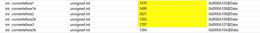
I want to read three different signals in three different moments. I have 3 PWM shifted 120 degrees (3 phase). In each PWM I have defined a CMPB to start one ADC conversion. When it finish, it should fire a interruption. However:

-The ADC conversion triggers all the interruptions, I can not assign each ADC with each interruption. I should have three interruptions (one per phase) in one cycle: One from ADC conversion A, other from ADC conversion B and the last one from ADC conversion C, but I am having many more per cycle.

-Maybe, I am firing all the ADC with one phase when they should work in pairs: ADC conversion A and phase A, ADC conversion B and phase B, ADC conversion C and phase C.

How can I solve this?

Very thank for your attention and your time.

Best regards,

Álvaro

  • Álvaro,

    Can you confirm that your ADCINTSOCSEL1 and ADCINTSOCSEL2 registers are cleared to 0? These registers are used to cross-trigger ADC SOCs.

    If this is not the issue, please share the ADC configurations for your three SOCs.

    -Tommy

  • Very thanks for your answer. ADCINTSOCSEL1 and ADCINTSOCSEL2 registers were the problem. I was using "AdcOffsetSelfCal();" which is a function created by TI team and they put these registers set to 1.´The problem of using some code which you did not programm.

  • I still having a problem. I have modified the code as you recommended, but when the DSP read my signal, it does not read a logical value (I am working at 60 kHz):

    I set a 0,5 duty cycle in each PWM (I have 3, shifted 120 degrees). In the picture 2, we can see the currents that I want to control. I want to read the value in the middle of the climb in each phase (in the middle of the high PWM). So, I set: CMPB=dutyx*750. I attach the PWMs, to show that the converter works.

    So I expected a similar values between phases (2000 aprox), but I get the values that appear in the picture 1 (without "b", the pins with "b" are fedeed by a source) (they are stable, so I think that it is not a duration of conversion and calculation problem). In picture 1, corrientefase1=ADCRESULT0, corrientefase1b=ADCRESULT1, corrientefase2=ADCINTRESULT2, corrientefase2b=ADCINTRESULT3, corrientefase3=ADCINTRESULT4,corrientefase3b=ADCINTRESULT5.

    What can be the problem? How can I solve it? (I attach my fixed code)

    Very thaks for your time.

    Best regards, 

    Álvaro

    //PICHICA, TIENES QEU ORDENAR EN STRUCTS: VER QEU VARIABLES GLOBALES Y CUALES GLOBALES
    //CALIBRAR Lectura de ADC
    //Comprbar que con fuente externa como referencia regula. NO LO HACE
    //Comprobar cuando dispara en modo BOOST
    //Las funciones de tranferencia del modo Boost y Buck son distintas. Por eso dos controladores. Si queremos usar solo 1, el modo buck se hace lento.
    //El ancho de banda del convertidor es donde corta con 0 en las ganancias. Revisar para ver que cubre.
    //###########################################################################
    //
    // FILE:   Example_2806xAdcSoc.c
    //
    // TITLE:  Buck-Boost Controller
    //
    // Control de un convertidor bidireccional buck-boost, con una funci�n de
    // transferencia XXX.
    //###########################################################################
    // $TI Release: F2806x Support Library v2.04.00.00 $
    // $Release Date: Sun Sep 29 07:33:29 CDT 2019 $
    // $Copyright:
    // Copyright (C) 2009-2019 Texas Instruments Incorporated - http://www.ti.com/
    //
    // Redistribution and use in source and binary forms, with or without 
    // modification, are permitted provided that the following conditions 
    // are met:
    // 
    //   Redistributions of source code must retain the above copyright 
    //   notice, this list of conditions and the following disclaimer.
    // 
    //   Redistributions in binary form must reproduce the above copyright
    //   notice, this list of conditions and the following disclaimer in the 
    //   documentation and/or other materials provided with the   
    //   distribution.
    // 
    //   Neither the name of Texas Instruments Incorporated nor the names of
    //   its contributors may be used to endorse or promote products derived
    //   from this software without specific prior written permission.
    // 
    // THIS SOFTWARE IS PROVIDED BY THE COPYRIGHT HOLDERS AND CONTRIBUTORS 
    // "AS IS" AND ANY EXPRESS OR IMPLIED WARRANTIES, INCLUDING, BUT NOT 
    // LIMITED TO, THE IMPLIED WARRANTIES OF MERCHANTABILITY AND FITNESS FOR
    // A PARTICULAR PURPOSE ARE DISCLAIMED. IN NO EVENT SHALL THE COPYRIGHT 
    // OWNER OR CONTRIBUTORS BE LIABLE FOR ANY DIRECT, INDIRECT, INCIDENTAL, 
    // SPECIAL, EXEMPLARY, OR CONSEQUENTIAL DAMAGES (INCLUDING, BUT NOT 
    // LIMITED TO, PROCUREMENT OF SUBSTITUTE GOODS OR SERVICES; LOSS OF USE,
    // DATA, OR PROFITS; OR BUSINESS INTERRUPTION) HOWEVER CAUSED AND ON ANY
    // THEORY OF LIABILITY, WHETHER IN CONTRACT, STRICT LIABILITY, OR TORT 
    // (INCLUDING NEGLIGENCE OR OTHERWISE) ARISING IN ANY WAY OUT OF THE USE 
    // OF THIS SOFTWARE, EVEN IF ADVISED OF THE POSSIBILITY OF SUCH DAMAGE.
    // $
    //###########################################################################
    
    //
    // Included Files
    //
    #include "DSP28x_Project.h"     // Device Headerfile and Examples Include File
    
    //
    // Function Prototypes
    //
    __interrupt void adc_isr1(void);
    __interrupt void adc_isr2(void);
    __interrupt void adc_isr3(void);
    void Adc_Config(void);
    void InitEPwm1Example(void);
    void InitEPwm2Example(void);
    void InitEPwm3Example(void);
    //
    // Globals
    //
    
    Uint16 ConversionCount;
    Uint16 Voltage;
    Uint16 Voltagereferencia;
    Uint32  EPwm1TimerIntCount;
    Uint32  EPwm2TimerIntCount;
    Uint32  EPwm3TimerIntCount;
    #define EPWM1_MIN_DB   0x0064
    #define EPWM2_MIN_DB   0x0064
    #define EPWM3_MIN_DB   0x0064
    
    float duty1 = 0.5;
    float dutyold1=0;
    float dutyoldold1=0;
    float il1=0;
    float ilold1=0;
    float iloldold1=0;
    float duty2 = 0.5;
    float dutyold2=0;
    float dutyoldold2=0;
    float il2=0;
    float ilold2=0;
    float iloldold2=0;
    float referencia=2000;
    const int Offset=0;
    float duty3 = 0.5;
    float dutyold3=0;
    float dutyoldold3=0;
    float il3=0;
    float ilold3=0;
    float iloldold3=0;
    //Variables comprobaci�n funcionamiento.
    float dutyVirtual=0.5;
    float errorcorriente=0;
    unsigned int corrientefase1;
    unsigned int corrientefase2;
    unsigned int corrientefase3;
    unsigned int corrientefase1b;
    unsigned int corrientefase2b;
    unsigned int corrientefase3b;
    //
    // Main
    // 
    void main(void)
    {
        //
        // Step 1. Initialize System Control:
        // PLL, WatchDog, enable Peripheral Clocks
        // This example function is found in the F2806x_SysCtrl.c file.
        //
        InitSysCtrl();
    
        //
        // Step 2. Initialize GPIO:
    
        //I launch the pins to measure timings and see when are they fired.
    
        EALLOW;
        GpioCtrlRegs.GPAMUX1.bit.GPIO12=0x0000;
        GpioCtrlRegs.GPAPUD.bit.GPIO12=0x0000;
        GpioCtrlRegs.GPADIR.bit.GPIO12=0x0001;
        GpioCtrlRegs.GPAQSEL1.bit.GPIO12=0x0000;
        GpioCtrlRegs.GPAMUX2.bit.GPIO18=0x0000;
        GpioCtrlRegs.GPAPUD.bit.GPIO18=0x0000;
        GpioCtrlRegs.GPADIR.bit.GPIO18=0x0001;
        GpioCtrlRegs.GPAQSEL2.bit.GPIO18=0x0000;
        GpioCtrlRegs.GPAMUX2.bit.GPIO22=0x0000;
        GpioCtrlRegs.GPAPUD.bit.GPIO22=0x0000;
        GpioCtrlRegs.GPADIR.bit.GPIO22=0x0001;
        GpioCtrlRegs.GPAQSEL2.bit.GPIO22=0x0000;
        GpioCtrlRegs.GPAMUX2.bit.GPIO20=0x0000;
        GpioCtrlRegs.GPAPUD.bit.GPIO20=0x0000;
        GpioCtrlRegs.GPADIR.bit.GPIO20=0x0001;
        GpioCtrlRegs.GPAQSEL2.bit.GPIO20=0x0000;
        GpioCtrlRegs.GPAMUX1.bit.GPIO14=0x0000;
        GpioCtrlRegs.GPAPUD.bit.GPIO14=0x0000;
        GpioCtrlRegs.GPADIR.bit.GPIO14=0x0001;
        GpioCtrlRegs.GPAQSEL1.bit.GPIO14=0x0000;
        GpioCtrlRegs.GPAMUX2.bit.GPIO21=0x0000;
        GpioCtrlRegs.GPAPUD.bit.GPIO21=0x0000;
        GpioCtrlRegs.GPADIR.bit.GPIO21=0x0001;
        GpioCtrlRegs.GPAQSEL2.bit.GPIO21=0x0000;
        GpioCtrlRegs.GPAMUX2.bit.GPIO23=0x0000;
        GpioCtrlRegs.GPAPUD.bit.GPIO23=0x0000;
        GpioCtrlRegs.GPADIR.bit.GPIO23=0x0001;
        GpioCtrlRegs.GPAQSEL2.bit.GPIO23=0x0000;
        EDIS;
    
        InitEPwm1Gpio();
        InitEPwm2Gpio();
        InitEPwm3Gpio();
    
        //
        // Step 3. Clear all interrupts and initialize PIE vector table:
        // Disable CPU interrupts
        //
        DINT;
    
        //
        // Initialize the PIE control registers to their default state.
        // The default state is all PIE interrupts disabled and flags
        // are cleared.
        // This function is found in the F2806x_PieCtrl.c file.
        //
        InitPieCtrl();
    
        //
        // Disable CPU interrupts and clear all CPU interrupt flags:
        //
        IER = 0x0000;
        IFR = 0x0000;
    
        //
        // Initialize the PIE vector table with pointers to the shell Interrupt
        // Service Routines (ISR).
        // This will populate the entire table, even if the interrupt
        // is not used in this example.  This is useful for debug purposes.
        // The shell ISR routines are found in F2806x_DefaultIsr.c.
        // This function is found in F2806x_PieVect.c.
        //
        InitPieVectTable();
    
    
        //
        // Interrupts that are used in this example are re-mapped to
        // ISR functions found within this file.
        //
        EALLOW;  // This is needed to write to EALLOW protected register
        PieVectTable.rsvd10_1 = &adc_isr1;
        EDIS;    // This is needed to disable write to EALLOW protected registers
    
    
        EALLOW;  // This is needed to write to EALLOW protected register
        PieVectTable.rsvd10_2 = &adc_isr2;
        EDIS;
    
    
        EALLOW;  // This is needed to write to EALLOW protected register
        PieVectTable.ADCINT3 = &adc_isr3;
        EDIS;
    
    
        //
        // Step 4. Initialize all the Device Peripherals:
        // This function is found in F2806x_InitPeripherals.c
        // InitPeripherals(); // Not required for this example
        //
        InitAdc();  // For this example, init the ADC
        //AdcOffsetSelfCal();
    
        //Necesario "desconfigurar" para que funcione, ya que se activan en funci�n anterior
        EALLOW;
        AdcRegs.ADCINTSOCSEL1.bit.SOC0  = 0;    // ADCINT2 NO starts SOC0-7
        AdcRegs.ADCINTSOCSEL1.bit.SOC1  = 0;
        AdcRegs.ADCINTSOCSEL1.bit.SOC2  = 0;
        AdcRegs.ADCINTSOCSEL1.bit.SOC3  = 0;
        AdcRegs.ADCINTSOCSEL1.bit.SOC4  = 0;
        AdcRegs.ADCINTSOCSEL1.bit.SOC5  = 0;
        AdcRegs.ADCINTSOCSEL1.bit.SOC6  = 0;
        AdcRegs.ADCINTSOCSEL1.bit.SOC7  = 0;
        AdcRegs.ADCINTSOCSEL2.bit.SOC8  = 0;    // ADCINT1 NO starts SOC8-15
        AdcRegs.ADCINTSOCSEL2.bit.SOC9  = 0;
        AdcRegs.ADCINTSOCSEL2.bit.SOC10 = 0;
        AdcRegs.ADCINTSOCSEL2.bit.SOC11 = 0;
        AdcRegs.ADCINTSOCSEL2.bit.SOC12 = 0;
        AdcRegs.ADCINTSOCSEL2.bit.SOC13 = 0;
        AdcRegs.ADCINTSOCSEL2.bit.SOC14 = 0;
        AdcRegs.ADCINTSOCSEL2.bit.SOC15 = 0;
        EDIS;
        //
        // Step 5. User specific code, enable interrupts:
        //
    
        //
        // Enable ADCINT1 in PIE
        //
        PieCtrlRegs.PIEIER10.bit.INTx1 = 1; // Enable INT 1.1 in the PIE
    
        PieCtrlRegs.PIEIER10.bit.INTx2 = 1; // Enable INT 10.4 in the PIE
    
    
        PieCtrlRegs.PIEIER10.bit.INTx3 = 1; // Enable INT 10.3 in the PIE
    
        IER |= M_INT10; 					   // Enable CPU Interrupt 10
        //IER |= M_INT1;
        EINT;          					   // Enable Global interrupt INTM
        ERTM;          					   // Enable Global realtime interrupt DBGM
    
        EALLOW;
        SysCtrlRegs.PCLKCR0.bit.TBCLKSYNC = 0;
        EDIS;
    
        InitEPwm1Example();
        InitEPwm2Example();
        InitEPwm3Example();
    
        EALLOW;
        SysCtrlRegs.PCLKCR0.bit.TBCLKSYNC = 1;
        EDIS;
    
        //
        // Configure ADC
        //
        EALLOW;
        AdcRegs.ADCCTL2.bit.ADCNONOVERLAP = 1; // Enable non-overlap mode
        
        //
        // ADCINT1 trips after AdcResults latch
        //
        AdcRegs.ADCCTL1.bit.INTPULSEPOS	= 1;
        
        AdcRegs.INTSEL1N2.bit.INT1E     = 1;  // Enabled ADCINT1
        AdcRegs.INTSEL1N2.bit.INT1CONT  = 0;  // Disable ADCINT1 Continuous mode
    
    
        AdcRegs.INTSEL1N2.bit.INT2E     = 1;  // Enabled ADCINT2
        AdcRegs.INTSEL1N2.bit.INT2CONT  = 0;  // Disable ADCINT2 Continuous mode


        AdcRegs.INTSEL3N4.bit.INT3E     = 1;  // Enabled ADCINT3
        AdcRegs.INTSEL3N4.bit.INT3CONT  = 0;  // Disable ADCINT3 Continuous mode
    /*
        //
        // setup EOC1 to trigger ADCINT1 to fire
        //
        //SEQUENTIAL MODE
        AdcRegs.INTSEL1N2.bit.INT1SEL 	= 1;
        AdcRegs.INTSEL1N2.bit.INT2SEL   = 2;
        AdcRegs.INTSEL3N4.bit.INT3SEL   = 3;
    
        //Sequential mode
        AdcRegs.ADCSOC1CTL.bit.CHSEL    = 0;  // set SOC1 channel select to ADCINA0
    
        AdcRegs.ADCSOC2CTL.bit.CHSEL    = 1;  // set SOC2 channel select to ADCINA1
    
        AdcRegs.ADCSOC3CTL.bit.CHSEL    = 2;  // set SOC3 channel select to ADCINA2
    
          //
          //SEQUENTIAL
          // set SOC1 start trigger on EPWM1A, due to round-robin SOC0 converts
          // first then SOC1
          //
          AdcRegs.ADCSOC1CTL.bit.TRIGSEL  = 5;
    
    
          //
          // set SOC2 start trigger on EPWM2A, due to round-robin SOC0 converts
          // first then SOC1
          //
          AdcRegs.ADCSOC2CTL.bit.TRIGSEL  = 7;
    
          //
          // set SOC4 start trigger on EPWM3A, due to round-robin SOC0 converts
          // first then SOC1
          //
          AdcRegs.ADCSOC3CTL.bit.TRIGSEL  = 9;
    
    
          //
          // set SOC1 S/H Window to 7 ADC Clock Cycles, (6 ACQPS plus 1)
          //
    
          AdcRegs.ADCSOC1CTL.bit.ACQPS    = 6;
          //
          // set SOC0 S/H Window to 7 ADC Clock Cycles, (6 ACQPS plus 1)
          //
          AdcRegs.ADCSOC2CTL.bit.ACQPS    = 6;
    
         //
          // set SOC1 S/H Window to 7 ADC Clock Cycles, (6 ACQPS plus 1)
          //
          AdcRegs.ADCSOC3CTL.bit.ACQPS    = 6;
    
    */
    
        //SIMULTANEOUS MODE
        AdcRegs.ADCSAMPLEMODE.bit.SIMULEN0=1;
        AdcRegs.ADCSOC0CTL.bit.CHSEL    = 0;


        AdcRegs.ADCSAMPLEMODE.bit.SIMULEN2=1;
        AdcRegs.ADCSOC2CTL.bit.CHSEL    = 1;
    
    
        AdcRegs.ADCSAMPLEMODE.bit.SIMULEN4=1;
        AdcRegs.ADCSOC4CTL.bit.CHSEL    = 2;
    
        //SIMULTANEOUS MODE
        //Recomendaci�n del colega de TI. Ojo que al usar SIMULEN, el SOC1 corresponde con EOC1 y as�.
        AdcRegs.INTSEL1N2.bit.INT1SEL   = 1;  // EOC0 triggers INT1
        AdcRegs.INTSEL1N2.bit.INT2SEL   = 3;  // EOC2 triggers INT2
        AdcRegs.INTSEL3N4.bit.INT3SEL   = 5; // EOC4 triggers INT3


        // SIMULTANEOUS
        AdcRegs.ADCSOC0CTL.bit.TRIGSEL  = 5;
        AdcRegs.ADCSOC1CTL.bit.TRIGSEL  = 0;  //make sure that the odd SOCs are disabled.
        AdcRegs.ADCSOC2CTL.bit.TRIGSEL  = 7;
        AdcRegs.ADCSOC3CTL.bit.TRIGSEL  = 0;
        AdcRegs.ADCSOC4CTL.bit.TRIGSEL  = 9;
        AdcRegs.ADCSOC5CTL.bit.TRIGSEL  = 0;


        //  SIMULTANEOUS
        AdcRegs.ADCSOC0CTL.bit.ACQPS    = 0x0006;
        AdcRegs.ADCSOC2CTL.bit.ACQPS    = 0x0006;
        AdcRegs.ADCSOC4CTL.bit.ACQPS    = 0x0006;
    
        EDIS;
    
    
        for(;;)
        {
            //This Code is for showing when should the DSP read the value
            if ( AdcRegs.ADCSOCFLG1.bit.SOC0 ==1)
            {
                GpioDataRegs.GPASET.bit.GPIO20=0x0001;
            }
            else
            {
                GpioDataRegs.GPACLEAR.bit.GPIO20=0x0001;
            }
            if ( AdcRegs.ADCSOCFLG1.bit.SOC1 ==1)
            {
                GpioDataRegs.GPASET.bit.GPIO14=0x0001;
            }
            else
            {
                GpioDataRegs.GPACLEAR.bit.GPIO14=0x0001;
            }
            if ( AdcRegs.ADCSOCFLG1.bit.SOC2 ==1)
            {
                GpioDataRegs.GPASET.bit.GPIO21=0x0001;
            }
            else
            {
                GpioDataRegs.GPACLEAR.bit.GPIO21=0x0001;
            }
            if ( AdcRegs.ADCSOCFLG1.bit.SOC4 ==1)
            {
                GpioDataRegs.GPASET.bit.GPIO23=0x0001;
            }
            else
            {
                GpioDataRegs.GPACLEAR.bit.GPIO23=0x0001;
            }
        }
    }
    
    //
    // adc_isr - 
    //
    __interrupt void
    adc_isr1(void)
    {
        GpioDataRegs.GPASET.bit.GPIO18=0x0001;
        //CONTROL FUNCTION
        iloldold1=ilold1;
        ilold1=il1;
        //corrientefase1=AdcResult.ADCRESULT1;
        //il1 = (referencia-(AdcResult.ADCRESULT1-Offset))*0.00081;
        // SIMULTANEO
        il1 = (referencia-(AdcResult.ADCRESULT0-Offset))*0.00081;
        corrientefase1=AdcResult.ADCRESULT0;
        corrientefase1b=AdcResult.ADCRESULT1;
        //OJO CAMBIAR VALORES CON MODO SIMULTANEO
        //il1 = (AdcResult.ADCRESULT1-(AdcResult.ADCRESULT0-Offset))*0.00081;
        errorcorriente=il1;
        dutyoldold1=dutyold1;
        dutyold1=duty1;
        //Buck control
        duty1 = 0.0007876*il1+0.0001147*ilold1-0.0006729*iloldold1+0.1743*dutyold1+0.8257*dutyoldold1;
        //Boost control Prueba
        //duty1   = 0.0008398*il1+0.0001147*ilold1-0.0007251*iloldold1+0.1743*dutyold1+0.8257*dutyoldold1;
    
        if (duty1 < 0.1)
        {
            duty1 = 0.1;
        }
        if (duty1 > 0.9)
        {
            duty1 = 0.9;
        }
    
        EPwm1Regs.CMPA.half.CMPA = (Uint16)(duty1*1500); //duty1*1500
    
        EPwm1Regs.CMPB=(Uint16)(duty1*750+EPWM1_MIN_DB); //duty1*750
    
        //
        // Clear ADCINT1 flag reinitialize for next SOC
        //
        AdcRegs.ADCINTFLGCLR.bit.ADCINT1 = 1;
        
        PieCtrlRegs.PIEACK.all = PIEACK_GROUP10;   // Acknowledge interrupt to PIE
        GpioDataRegs.GPACLEAR.bit.GPIO18=0x0001;
        return;
    }
    
    __interrupt void
    adc_isr2(void)
    {
        GpioDataRegs.GPASET.bit.GPIO22=0x0001;
        //CONTROL FUNCTION
        iloldold2=ilold2;
        ilold2=il2;
        //corrientefase2=AdcResult.ADCRESULT2;
        //il2 = (referencia-(AdcResult.ADCRESULT2-Offset))*0.00081;
        // SIMULTANEO
        il2 = (referencia-(AdcResult.ADCRESULT2-Offset))*0.00081;
        corrientefase2=AdcResult.ADCRESULT2;
        corrientefase2b=AdcResult.ADCRESULT3;
        //OJO CAMBIAR VALORES CON MODO SIMULTANEO
        //il2 = (AdcResult.ADCRESULT2-(AdcResult.ADCRESULT3-Offset))*0.00081;
    
        dutyoldold2=dutyold2;
        dutyold2=duty2;
        //duty2 = 0.0007876*il2+0.0001147*ilold2-0.0006729*iloldold2+0.1743*dutyold2+0.8257*dutyoldold2;
        duty2=0.5;
        if (duty2 < 0.1)
        {
            duty2 = 0.1;
        }
        if (duty2 > 0.9)
        {
            duty2 = 0.9;
        }
    
        EPwm2Regs.CMPA.half.CMPA = (Uint16)(duty2*1500);
    
        EPwm2Regs.CMPB=(Uint16)(duty2*750+EPWM2_MIN_DB);
    
        //
        // Clear ADCINT1 flag reinitialize for next SOC
        //
        AdcRegs.ADCINTFLGCLR.bit.ADCINT2 = 1;
    
        PieCtrlRegs.PIEACK.all = PIEACK_GROUP10;   // Acknowledge interrupt to PIE
        GpioDataRegs.GPACLEAR.bit.GPIO22=0x0001;
        return;
    }


    __interrupt void
    adc_isr3(void)
    {
        GpioDataRegs.GPASET.bit.GPIO12=0x0001;
        //CONTROL FUNCTION
        iloldold3=ilold3;
        ilold3=il3;
        //corrientefase3=AdcResult.ADCRESULT3;
        //il3 = (referencia-(AdcResult.ADCRESULT3-Offset))*0.00081;
        // SIMULTANEO
        il3 = (referencia-(AdcResult.ADCRESULT4-Offset))*0.00081;
        corrientefase3=AdcResult.ADCRESULT4;
        corrientefase3b=AdcResult.ADCRESULT5;
        //OJO CAMBIAR VALORES CON MODO SIMULTANEO
        //il3 = (AdcResult.ADCRESULT4-(AdcResult.ADCRESULT5-Offset))*0.00081; //Ojo que hay que a�adirle el offset a la entrada
    
        dutyoldold3=dutyold3;
        dutyold3=duty3;
        //duty3 = 0.0007876*il3+0.0001147*ilold3-0.0006729*iloldold3+0.1743*dutyold3+0.8257*dutyoldold3;
        duty3=0.5;
        if (duty3 < 0.1)
        {
            duty3 = 0.1;
        }
        if (duty3 > 0.9)
        {
            duty3 = 0.9;
        }
    
        EPwm3Regs.CMPA.half.CMPA = (Uint16)(duty3*1500);
    
        EPwm3Regs.CMPB=(Uint16)(duty3*750+EPWM3_MIN_DB);
    
        //
        // Clear ADCINT3 flag reinitialize for next SOC
        //
        AdcRegs.ADCINTFLGCLR.bit.ADCINT3 = 1;
    
        PieCtrlRegs.PIEACK.all = PIEACK_GROUP10;   // Acknowledge interrupt to PIE grupo 10
        GpioDataRegs.GPACLEAR.bit.GPIO12=0x0001;
        return;
    }
    
    void
    InitEPwm1Example()
    {
        EPwm1Regs.ETSEL.bit.SOCAEN  = 1;        // Enable SOC on A group
        EPwm1Regs.ETSEL.bit.SOCASEL = 6;        // Select SOC from CMPB on upcount
        EPwm1Regs.ETPS.bit.SOCAPRD  = 1;        // Generate pulse on 1st event
    
        EPwm1Regs.TBPRD = 1499;                        // Set timer period
        EPwm1Regs.TBPHS.half.TBPHS = 0x0000;           // Phase is a 0
        EPwm1Regs.TBCTR = 0x0000;                      // Clear counter
    
        //
        // Setup TBCLK
        //
        EPwm1Regs.TBCTL.bit.CTRMODE = TB_COUNT_UP; // Count up
        EPwm1Regs.TBCTL.bit.PHSEN = TB_DISABLE;        // Disable phase loading
        EPwm1Regs.TBCTL.bit.HSPCLKDIV = TB_DIV1;       // Clock ratio to SYSCLKOUT
        EPwm1Regs.TBCTL.bit.CLKDIV = TB_DIV1;
        EPwm1Regs.TBCTL.bit.PRDLD = TB_SHADOW;
        EPwm1Regs.TBCTL.bit.SYNCOSEL = TB_CTR_ZERO;
    
    
        EPwm1Regs.CMPCTL.bit.SHDWAMODE = CC_SHADOW;    // Load registers every ZERO
        EPwm1Regs.CMPCTL.bit.SHDWBMODE = CC_SHADOW;
        EPwm1Regs.CMPCTL.bit.LOADAMODE = CC_CTR_ZERO;
        EPwm1Regs.CMPCTL.bit.LOADBMODE = CC_CTR_ZERO;
    
        //
        // Setup compare
        //
        EPwm1Regs.CMPA.half.CMPA = duty1*1500;
        EPwm1Regs.CMPB=750+EPWM1_MIN_DB;
        //
        // Set actions
        //
        EPwm1Regs.AQCTLA.bit.CAU = AQ_CLEAR;           // Set PWM1A on CAU
        EPwm1Regs.AQCTLA.bit.ZRO = AQ_SET;         // Clear PWM1A on CAD
    
        EPwm1Regs.AQCTLB.bit.CAU = AQ_SET;         // Clear PWM1B on CAU
        EPwm1Regs.AQCTLB.bit.ZRO = AQ_CLEAR;           // Set PWM1B on CAD
    
       //
        // Active Low PWMs - Setup Deadband
        //
        EPwm1Regs.DBCTL.bit.OUT_MODE = DB_FULL_ENABLE;
        EPwm1Regs.DBCTL.bit.POLSEL = DB_ACTV_HIC;
        EPwm1Regs.DBCTL.bit.IN_MODE = DBA_ALL;
        EPwm1Regs.DBRED = EPWM1_MIN_DB;
        EPwm1Regs.DBFED = EPWM1_MIN_DB;
    
    }
    
    void
    InitEPwm2Example()
    {
        EPwm2Regs.ETSEL.bit.SOCAEN  = 1;        // Enable SOC on A group
        EPwm2Regs.ETSEL.bit.SOCASEL = 6;        // Select SOC from CMPB on upcount
        EPwm2Regs.ETPS.bit.SOCAPRD  = 1;        // Generate pulse on 1st event
        EPwm2Regs.TBPRD = 1499;                        // Set timer period
        EPwm2Regs.TBPHS.half.TBPHS = 500;           // Phase is 0
        EPwm2Regs.TBCTR = 0x0000;                      // Clear counter
    
        //
        // Setup TBCLK
        //
        EPwm2Regs.TBCTL.bit.CTRMODE = TB_COUNT_UP; // Count up
        EPwm2Regs.TBCTL.bit.PHSEN = TB_ENABLE;        // Disable phase loading
        EPwm2Regs.TBCTL.bit.HSPCLKDIV = TB_DIV1;       // Clock ratio to SYSCLKOUT
        EPwm2Regs.TBCTL.bit.CLKDIV = TB_DIV1;
        EPwm2Regs.TBCTL.bit.PRDLD = TB_SHADOW;
        EPwm2Regs.TBCTL.bit.SYNCOSEL = TB_SYNC_IN;
    
    
        EPwm2Regs.CMPCTL.bit.SHDWAMODE = CC_SHADOW;    // Load registers every ZERO
        EPwm2Regs.CMPCTL.bit.SHDWBMODE = CC_SHADOW;
        EPwm2Regs.CMPCTL.bit.LOADAMODE = CC_CTR_ZERO;
        EPwm2Regs.CMPCTL.bit.LOADBMODE = CC_CTR_ZERO;
    
        //
        // Setup compare
        //
        EPwm2Regs.CMPA.half.CMPA = duty2*1500;
        EPwm2Regs.CMPB=750+EPWM2_MIN_DB;
    
        //
        // Set actions
        //
        EPwm2Regs.AQCTLA.bit.CAU = AQ_CLEAR;           // Set PWM1A on CAU
        EPwm2Regs.AQCTLA.bit.ZRO = AQ_SET;         // Clear PWM1A on CAD
    
        EPwm2Regs.AQCTLB.bit.CAU = AQ_SET;         // Clear PWM1B on CAU
        EPwm2Regs.AQCTLB.bit.ZRO = AQ_CLEAR;           // Set PWM1B on CAD
    
       //
        // Active Low PWMs - Setup Deadband
        //
        EPwm2Regs.DBCTL.bit.OUT_MODE = DB_FULL_ENABLE;
        EPwm2Regs.DBCTL.bit.POLSEL = DB_ACTV_HIC;
        EPwm2Regs.DBCTL.bit.IN_MODE = DBA_ALL;
        EPwm2Regs.DBRED = EPWM2_MIN_DB;
        EPwm2Regs.DBFED = EPWM2_MIN_DB;


    }
    
    //
    // InitEPwm3Example -
    //
    void
    InitEPwm3Example()
    {
        EPwm3Regs.ETSEL.bit.SOCAEN  = 1;        // Enable SOC on A group
        EPwm3Regs.ETSEL.bit.SOCASEL = 6;        // Select SOC from CMPB on upcount
        EPwm3Regs.ETPS.bit.SOCAPRD  = 1;        // Generate pulse on 1st event
        EPwm3Regs.TBPRD = 1499;                        // Set timer period
        EPwm3Regs.TBPHS.half.TBPHS = 1000;           // Phase is 0
        EPwm3Regs.TBCTR = 0x0000;                      // Clear counter
    
        //
        // Setup TBCLK
        //
        EPwm3Regs.TBCTL.bit.CTRMODE = TB_COUNT_UP; // Count up
        EPwm3Regs.TBCTL.bit.PHSEN = TB_ENABLE;        // Disable phase loading
        EPwm3Regs.TBCTL.bit.HSPCLKDIV = TB_DIV1;       // Clock ratio to SYSCLKOUT
        EPwm3Regs.TBCTL.bit.CLKDIV = TB_DIV1;
        EPwm3Regs.TBCTL.bit.PRDLD = TB_SHADOW;
        EPwm3Regs.TBCTL.bit.SYNCOSEL = TB_SYNC_IN;
    
    
        EPwm3Regs.CMPCTL.bit.SHDWAMODE = CC_SHADOW;    // Load registers every ZERO
        EPwm3Regs.CMPCTL.bit.SHDWBMODE = CC_SHADOW;
        EPwm3Regs.CMPCTL.bit.LOADAMODE = CC_CTR_ZERO;
        EPwm3Regs.CMPCTL.bit.LOADBMODE = CC_CTR_ZERO;
    
        //
        // Setup compare
        //
        EPwm3Regs.CMPA.half.CMPA = duty3*1500;
        EPwm3Regs.CMPB=750+EPWM3_MIN_DB;
    
        //
        // Set actions
        //
        EPwm3Regs.AQCTLA.bit.CAU = AQ_CLEAR;           // Set PWM1A on CAU
        EPwm3Regs.AQCTLA.bit.ZRO = AQ_SET;         // Clear PWM1A on CAD
    
        EPwm3Regs.AQCTLB.bit.CAU = AQ_SET;         // Clear PWM1B on CAU
        EPwm3Regs.AQCTLB.bit.ZRO = AQ_CLEAR;           // Set PWM1B on CAD
    
       //
        // Active Low PWMs - Setup Deadband
        //
        EPwm3Regs.DBCTL.bit.OUT_MODE = DB_FULL_ENABLE;
        EPwm3Regs.DBCTL.bit.POLSEL = DB_ACTV_HIC;
        EPwm3Regs.DBCTL.bit.IN_MODE = DBA_ALL;
        EPwm3Regs.DBRED = EPWM3_MIN_DB;
        EPwm3Regs.DBFED = EPWM3_MIN_DB;
    
    }
    //
    // End of File
    //


  • Álvaro,

    We are only able to provide guidance on specific device behavior at a module level and are therefore not able to debug and correct whole examples or programs. Please break down the problem into concise points of failure that we can address individually.

    For example, if you suspect that the ADC is not sampling at CMPB as desired, I recommend profiling both the CMPB trigger and ADC conversion. The CMPB trigger can be monitored by toggling an unused EPWM pin through AQCTL or through the external ADCSOCxO signal when CMPB is matched. The ADC conversion can be monitored by storing the EPWM TBCTR count or by toggling an unused GPIO in the ADC ISR.

    -Tommy

  • Very thanks for your time, I am going to try to explain myself very concrete. 

    One question is: Why is my ADC reading these values (they are variable, see picture) if I apply a constant value of 2.34 V with a constant source (first I apply 2.33 V, then I change to 2.34 V and the variable values appears)?

    I am using the same code.

    Very thanks for your time.

    Best regards, 

    Álvaro

  • Sorry, the step was from 2.24 V to 2.34 V

  • Other question.

    After the DSP read the values ( both of them, in simultaneous mode), I want to use them in the interruption, but they do make any effect in the code. I mean, I am reading the values, then in the interruption they should update my duty cycle value (I am using addition, subtractions and multiplications), but It does not work. When I do not use both values of the ADC (simultaneous), the duty cycle value update in the right way. Why can it happen? How can I solve it?

    Very thanks for your support. It is very important for me.

    Best regards,

    Álvaro

  • Álvaro,

    It looks to me like there may be some digital noise being injected at the board level. Are you activating some pin activity around the time the noise starts?

    I recommend placing an oscilloscope probe as close to the ADC pin as possible to determine if you can observe the noise directly.

    -Tommy

  • user6232444 said:
    Other question.

    After the DSP read the values ( both of them, in simultaneous mode), I want to use them in the interruption, but they do make any effect in the code. I mean, I am reading the values, then in the interruption they should update my duty cycle value (I am using addition, subtractions and multiplications), but It does not work. When I do not use both values of the ADC (simultaneous), the duty cycle value update in the right way. Why can it happen? How can I solve it?

    There is no logical linkage between the ADC configuration versus EPWM register updates. Are you sure that the ISR is being triggered?

  • I am sure that they are being triggering. I configured a GPIO pin in each interruption, and it toggles its value when it should do it.

  • I noticed that the noise appear and disappear depending on the operation point of the board. But I do not find the relationship, I mean, where the noise come from. How can I avoid this noise? Because this noise introduce some big instabilities.

    Very thanks for your attention, it is being very helpful.

    Best regards,

    Álvaro

  • user6232444 said:
    I noticed that the noise appear and disappear depending on the operation point of the board. But I do not find the relationship, I mean, where the noise come from. How can I avoid this noise? Because this noise introduce some big instabilities.

    We are limited in our ability to assist with debugging board issues that are not directly related to our devices.

    Generally speaking, noise is usually generated by a noisy component, unstable circuit design, or poor signal integrity (PCB routing).

  • user6232444 said:
    I am sure that they are being triggering. I configured a GPIO pin in each interruption, and it toggles its value when it should do it.

    I recommend setting a breakpoint in the ISR and observing the register updates as you single step through the code execution.

  • I have done it and I find that this expressioin is not well calculated:

    il2 = (AdcResult.ADCRESULT3-(AdcResult.ADCRESULT2-Offset))*0.00081;

    Where:

    il2 is a float

    Offset is a float

    AdcResult.ADCRESULTx are unsigned int.

    Can the mix of number types be a problem?

    Very thanks for your time.

    Best regards,

    Álvaro

  • Álvaro,

    Please try to provide details when outcomes deviate from expectations. We have no context for understanding how the evaluation of the equation has gone wrong. If the equation appears to have been evaluated using integer math, you can use typecasting to instruct the compiler to use floating point math instead.

    -Tommy