This thread has been locked.

If you have a related question, please click the "Ask a related question" button in the top right corner. The newly created question will be automatically linked to this question.

TMS320F280049: create sine wave using TMDXDOCK280049M

Part Number: TMS320F280049
Other Parts Discussed in Thread: TMDSCNCD280049C, C2000WARE

Hi there,

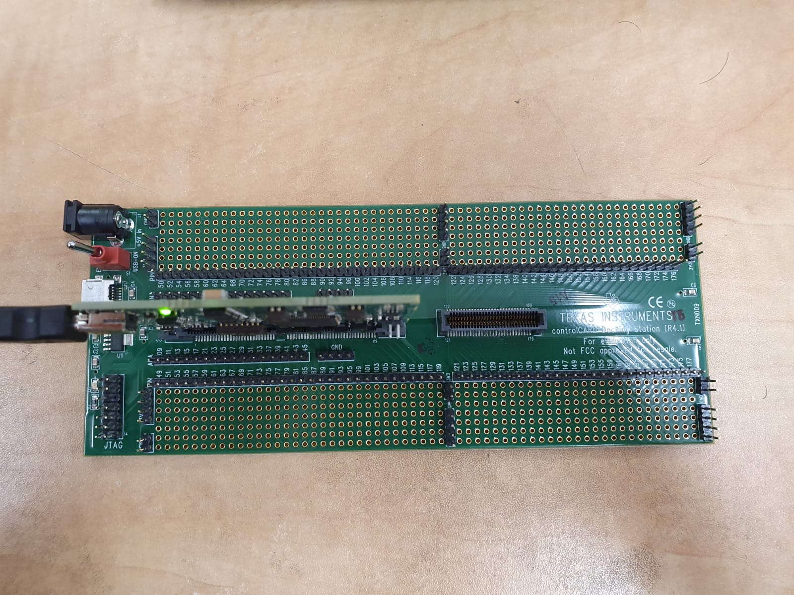
i am new to TI development kits, i got TMDXDOCK280049M  and i want to create sine wave with that kit but i dont know where to start.

there is a quick guide for it?

i didnt find any examples projects for that kit.

Best Regards

Michael

  • Michael,

    where did you fine a TMDXDOCK280049M? These haven't been sold for a little while. 

    Nonetheless, don't worry! They are basically identical to the TMDSCNCD280049C found here: http://www.ti.com/tool/TMDSCNCD280049C 

    You can find the User's Guide(UG) and software example in C2000Ware. 

    UG and Design files:  C:\ti\c2000\C2000Ware_2_01_00_00\boards\controlCARDs\TMDSCNCD280049M

    Software Examples:   C:\ti\c2000\C2000Ware_2_01_00_00\driverlib\f28004x\examples

    Regards,
    Cody 

  • Hi there,  thank you for the answer!

    i think that TMDXDOCK280049M are still being on sell on couple of sites online (digikey/mouser).

    i am trying to open a example project but i am facing a problem to connect the device.

    i also tried to change the JTAG speed, but it did not work, and when i am running a connection check i get this massege:

    " [Start: Texas Instruments XDS100v2 USB Debug Probe_0]

    Execute the command:

    %ccs_base%/common/uscif/dbgjtag -f %boarddatafile% -rv -o -F inform,logfile=yes -S pathlength -S integrity

    [Result]


    -----[Print the board config pathname(s)]------------------------------------

    C:\Users\Michael\AppData\Local\TEXASI~1\
        CCS\ccs930\0\0\BrdDat\testBoard.dat

    -----[Print the reset-command software log-file]-----------------------------

    This utility has selected a 100- or 510-class product.
    This utility will load the adapter 'jioserdesusb.dll'.

    An error occurred while soft opening the controller.

    -----[An error has occurred and this utility has aborted]--------------------

    This error is generated by TI's USCIF driver or utilities.

    The value is '-151' (0xffffff69).
    The title is 'SC_ERR_FTDI_OPEN'.

    The explanation is:
    One of the FTDI driver functions used during the connect
    returned bad status or an error. The cause may be one or
    more of: no XDS100 is plugged in, invalid XDS100 serial number,
    blank XDS100 EEPROM, missing FTDI drivers, faulty USB cable.
    Use the xds100serial command-line utility in the 'common/uscif'
    folder to verify the XDS100 can be located.

    [End: Texas Instruments XDS100v2 USB Debug Probe_0]   "

    Best regards

    Michael

  • Its very likely that you didn't connect power or a communications cable to the device. Can you provide a picture of your setup?

    Thanks,
    Cody

  • you where right i accidentally connect the cable to the power connection.

    unfortunately i still have a problem.

    when i test the connection i get the error below, (i changed JTAG couple of times but it still shows the error )

    "

    [Start: Texas Instruments XDS100v2 USB Debug Probe_0]

    Execute the command:

    %ccs_base%/common/uscif/dbgjtag -f %boarddatafile% -rv -o -F inform,logfile=yes -S pathlength -S integrity

    [Result]


    -----[Print the board config pathname(s)]------------------------------------

    C:\Users\Michael\AppData\Local\TEXASI~1\
        CCS\ccs930\0\0\BrdDat\testBoard.dat

    -----[Print the reset-command software log-file]-----------------------------

    This utility has selected a 100- or 510-class product.
    This utility will load the adapter 'jioserdesusb.dll'.
    The library build date was 'Nov 25 2019'.
    The library build time was '16:55:29'.
    The library package version is '8.4.0.00006'.
    The library component version is '35.35.0.0'.
    The controller does not use a programmable FPGA.
    The controller has a version number of '4' (0x00000004).
    The controller has an insertion length of '0' (0x00000000).
    This utility will attempt to reset the controller.
    This utility has successfully reset the controller.

    -----[Print the reset-command hardware log-file]-----------------------------

    The scan-path will be reset by toggling the JTAG TRST signal.
    The controller is the FTDI FT2232 with USB interface.
    The link from controller to target is direct (without cable).
    The software is configured for FTDI FT2232 features.
    The controller cannot monitor the value on the EMU[0] pin.
    The controller cannot monitor the value on the EMU[1] pin.
    The controller cannot control the timing on output pins.
    The controller cannot control the timing on input pins.
    The scan-path link-delay has been set to exactly '0' (0x0000).

    -----[The log-file for the JTAG TCLK output generated from the PLL]----------

    There is no hardware for programming the JTAG TCLK frequency.

    -----[Measure the source and frequency of the final JTAG TCLKR input]--------

    There is no hardware for measuring the JTAG TCLK frequency.

    -----[Perform the standard path-length test on the JTAG IR and DR]-----------

    This path-length test uses blocks of 64 32-bit words.

    The test for the JTAG IR instruction path-length failed.
    The JTAG IR instruction scan-path is stuck-at-ones.

    The test for the JTAG DR bypass path-length failed.
    The JTAG DR bypass scan-path is stuck-at-ones.

    -----[Perform the Integrity scan-test on the JTAG IR]------------------------

    This test will use blocks of 64 32-bit words.
    This test will be applied just once.

    Do a test using 0xFFFFFFFF.
    Scan tests: 1, skipped: 0, failed: 0
    Do a test using 0x00000000.
    Test 2 Word 0: scanned out 0x00000000 and scanned in 0xFFFFFFFF.
    Test 2 Word 1: scanned out 0x00000000 and scanned in 0xFFFFFFFF.
    Test 2 Word 2: scanned out 0x00000000 and scanned in 0xFFFFFFFF.
    Test 2 Word 3: scanned out 0x00000000 and scanned in 0xFFFFFFFF.
    Test 2 Word 4: scanned out 0x00000000 and scanned in 0xFFFFFFFF.
    Test 2 Word 5: scanned out 0x00000000 and scanned in 0xFFFFFFFF.
    Test 2 Word 6: scanned out 0x00000000 and scanned in 0xFFFFFFFF.
    Test 2 Word 7: scanned out 0x00000000 and scanned in 0xFFFFFFFF.
    The details of the first 8 errors have been provided.
    The utility will now report only the count of failed tests.
    Scan tests: 2, skipped: 0, failed: 1
    Do a test using 0xFE03E0E2.
    Scan tests: 3, skipped: 0, failed: 2
    Do a test using 0x01FC1F1D.
    Scan tests: 4, skipped: 0, failed: 3
    Do a test using 0x5533CCAA.
    Scan tests: 5, skipped: 0, failed: 4
    Do a test using 0xAACC3355.
    Scan tests: 6, skipped: 0, failed: 5
    Some of the values were corrupted - 83.3 percent.

    The JTAG IR Integrity scan-test has failed.

    -----[Perform the Integrity scan-test on the JTAG DR]------------------------

    This test will use blocks of 64 32-bit words.
    This test will be applied just once.

    Do a test using 0xFFFFFFFF.
    Scan tests: 1, skipped: 0, failed: 0
    Do a test using 0x00000000.
    Test 2 Word 0: scanned out 0x00000000 and scanned in 0xFFFFFFFF.
    Test 2 Word 1: scanned out 0x00000000 and scanned in 0xFFFFFFFF.
    Test 2 Word 2: scanned out 0x00000000 and scanned in 0xFFFFFFFF.
    Test 2 Word 3: scanned out 0x00000000 and scanned in 0xFFFFFFFF.
    Test 2 Word 4: scanned out 0x00000000 and scanned in 0xFFFFFFFF.
    Test 2 Word 5: scanned out 0x00000000 and scanned in 0xFFFFFFFF.
    Test 2 Word 6: scanned out 0x00000000 and scanned in 0xFFFFFFFF.
    Test 2 Word 7: scanned out 0x00000000 and scanned in 0xFFFFFFFF.
    The details of the first 8 errors have been provided.
    The utility will now report only the count of failed tests.
    Scan tests: 2, skipped: 0, failed: 1
    Do a test using 0xFE03E0E2.
    Scan tests: 3, skipped: 0, failed: 2
    Do a test using 0x01FC1F1D.
    Scan tests: 4, skipped: 0, failed: 3
    Do a test using 0x5533CCAA.
    Scan tests: 5, skipped: 0, failed: 4
    Do a test using 0xAACC3355.
    Scan tests: 6, skipped: 0, failed: 5
    Some of the values were corrupted - 83.3 percent.

    The JTAG DR Integrity scan-test has failed.

    [End: Texas Instruments XDS100v2 USB Debug Probe_0]  

    "

    thank you

    Michael

  • Ok, can you pleasen provide an image of your setup, or describe what cables you have connected? Please be sure to include what connectors the USB cables are connected to.

    Thanks,
    Cody

  • Hi, thank you for the answer

    Best Regards

    Michael

  • Michael,

    You have connected to and powered the embedded XDS100v2 emulator. However, you have not powered the C2000 device. Please connect a power supply to J1 or a USB cable to J17 of the docking station to provide power to the C2000 device.

    This design is used in many high-voltage system kits, so to protect user's computers we have implemented isolation between the Emulator and the C2000 device. Because of this they don't share the same power supply, and you will need to connect two USB cables, one for the emulator and one for the C2000 device.

    Regards,
    Cody 

  • Hi,

    its works,thank you.

    I have couple of questions regarding to the sine wave generation.

    i am using an example project dac_ex1_enable (exmp for TMDSCNCD280049C):

    • what is a shadow value (// DAC Value Register - Shadow)?
    • I cant find  ADCINB3  at the attached schematic and why there is a need to a reference voltage?                                            .
    •                                                                                  "! \b External \b Connections \n
                                                                                        //!  - When the DAC reference is set to VDAC, an external reference voltage
                                                                                        //!    must be applied to the VDAC pin. This can be accomplished by connecting a
                                                                                        //!    jumper wire from 3.3V to ADCINB3."
    • i asumme that the output is DACA, is it right?

    the code:

    #include "F28x_Project.h"
    //
    // Globals
    //
    volatile struct DAC_REGS* DAC_PTR[3] = {0x0,&DacaRegs,&DacbRegs};
    //uint16_t dacval = 2048;

    //
    // Defines
    //
    #define REFERENCE_VDAC      0
    #define REFERENCE_VREF      1
    #define DACA         1
    #define DACB         2

    #define REFERENCE            REFERENCE_VDAC
    #define DAC_NUM                DACA

    //
    // Function Prototypes
    //
    void configureDAC(uint16_t dac_num);


    #define PERIOD 120
     static const uint16_t D_Val[PERIOD] = {  0x7ff, 0x86a, 0x8d5, 0x93f, 0x9a9, 0xa11, 0xa78, 0xadd, 0xb40, 0xba1,
                                              0xbff, 0xc5a, 0xcb2, 0xd08, 0xd59, 0xda7, 0xdf1, 0xe36, 0xe77, 0xeb4,
                                              0xeec, 0xf1f, 0xf4d, 0xf77, 0xf9a, 0xfb9, 0xfd2, 0xfe5, 0xff3, 0xffc,
                                              0xfff, 0xffc, 0xff3, 0xfe5, 0xfd2, 0xfb9, 0xf9a, 0xf77, 0xf4d, 0xf1f,
                                              0xeec, 0xeb4, 0xe77, 0xe36, 0xdf1, 0xda7, 0xd59, 0xd08, 0xcb2, 0xc5a,
                                              0xbff, 0xba1, 0xb40, 0xadd, 0xa78, 0xa11, 0x9a9, 0x93f, 0x8d5, 0x86a,
                                              0x7ff, 0x794, 0x729, 0x6bf, 0x655, 0x5ed, 0x586, 0x521, 0x4be, 0x45d,
                                              0x3ff, 0x3a4, 0x34c, 0x2f6, 0x2a5, 0x257, 0x20d, 0x1c8, 0x187, 0x14a,
                                              0x112, 0xdf, 0xb1, 0x87, 0x64, 0x45, 0x2c, 0x19, 0xb, 0x2,
                                              0x0, 0x2, 0xb, 0x19, 0x2c, 0x45, 0x64, 0x87, 0xb1, 0xdf,
                                              0x112, 0x14a, 0x187, 0x1c8, 0x20d, 0x257, 0x2a5, 0x2f6, 0x34c, 0x3a4,
                                              0x3ff, 0x45d, 0x4be, 0x521, 0x586, 0x5ed, 0x655, 0x6bf, 0x729, 0x794
                                            };


    //
    // Main
    //
    void main(void)
    {
        //
        // Initialize System Control:
        // PLL, WatchDog, enable Peripheral Clocks
        //
        InitSysCtrl();

        //
        // Disable CPU interrupts
        //
        DINT;

        //
        // Initialize the PIE control registers to their default state.
        // The default state is all PIE interrupts disabled and flags are cleared.
        //
        InitPieCtrl();

        //
        // Clear all interrupts and initialize PIE vector table:
        //
        IER = 0x0000;
        IFR = 0x0000;
        InitPieVectTable();

        //
        // Configure DAC
        //
        configureDAC(DAC_NUM);


        int i=0;


        while(1)
        {


                while(i<PERIOD)
                {
                     DAC_PTR[DAC_NUM]->DACVALS.all = D_Val[i];
                     DELAY_US(2);
                    i++;
                }
                i=0;

        }
    }


    //
    // configureDAC - Configure specified DAC output
    //
    void configureDAC(uint16_t dac_num)
    {
        EALLOW;
        DAC_PTR[dac_num]->DACCTL.bit.DACREFSEL = REFERENCE;
        DAC_PTR[dac_num]->DACOUTEN.bit.DACOUTEN = 1;
        DAC_PTR[dac_num]->DACVALS.all = 0;
        DELAY_US(10); // Delay for buffered DAC to power up
        EDIS;
    }

    //
    // End of File
    //

    the scematic:

    file:///C:/ti/c2000/C2000Ware_2_01_00_00/boards/controlCARDs/TMDSCNCD280049C/A/TMDSCNCD28004x_RevA_120cCARD_pinout.pdf

    Thank you very much!

    Michael

  • Michael,

    a shadow value is the next value to be loaded into a register after a set event. For example the DACHVALS register, see the register description below. This was taken from the Technical Reference Manual.

    "

    High DAC shadow value. When COMPDACCTL[DACSOURCE]=0,
    the value of DACHVALS is loaded into DACHVALA on the trigger
    signal selected by COMPDACCTL[SWLOADSEL].

    "

    I was unable to open the schematic you attached, so I opened the one included in C2000Ware for the F280049C controlCARD. ADCINB3 was shortened to B3, to make the schematic symbol more clean.

    Yes, there are two DAC outputs DACA and DACB, in the schematic these are called DACx_OUT.

    Regards,
    Cody 

  • hi thank you, it is working!

    by the way i notich that every time that i plug out the card i need to flash the code again.. is it normal?

    best regards

    Michael

  • Michael no that is not normal.

    You either have the Boot mode configuration wrong, or you are loading the code into RAM not Flash.

    Please check that S1 is set to pull GPIO24 and GPIO32 high. If that is correct, and you are loading your code into flash, then you probably have a bug in your code.

    Regards,
    Cody 

  • HI Cody thank you for the reply,

    i am not sure what it dose it mean S1 is set to pull GPIO24 and GPIO32 high ,

    as i understood is to measure voltage  at gpio 32 - the voltage is low as well as at gpio 24 - the switch is on usb - on mode.

    this is my first time to use TI product, so if you can explain me in more details it will be great , thank you very much!

    Michael


  • Michael,

    I was referring to S1 of the controlCARD, not the docking station. This switch controls what boot mode is used when the device is powered on.

    GPIO 24 and 32 should be logic high.

    Regards,
    Cody 

  • thank you for the answer,

    both GPIO24 and GPIO 32 are not on logic 1 in any position that i turn the switch.

    the code is the same as mention couple of massages before - can you see any problem in it?

    thank you,

    Michael

  • Michael, 

    check if you have configured the GPIOs as output and set "0" in the GPxDAT register.

    However, your code shouldn't affect this. During startup your code is not yet running. At this time the device reads the voltage on these two GPIOs and determines what boot mode to select. If both GPIOs are logic high then it will boot to flash.

    Regards,
    Cody 

  • Hi can you please guide me how to do it? (i didnt find info on that at google)

    "check if you have configured the GPIOs as output and set "0" in the GPxDAT register"

    Best Regards

    Michael

  • Michael,

    please read the documentation for GPIOs found in the TRM. Specifically the following registers should help: GPxDIR, GPxDAT, GPxMUX1, GPxMUX2.

    once you understand what each register is doing you can verify your code.

    Regards,
    Cody 

  • Thank you very much for your help Cody!

  • Great, glad I could help. Can I close this thread?

    You can always start another if you have more questions.


    Regards,
    Cody