Part Number: TMS320F280049
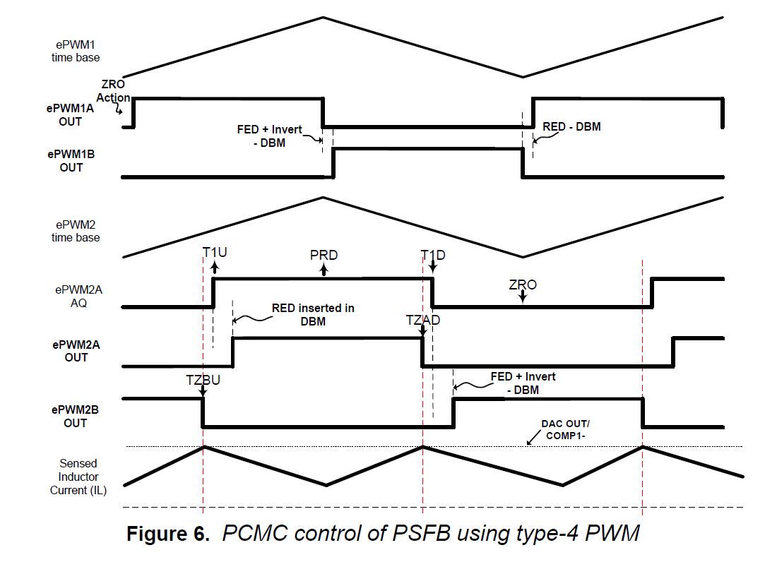
I am having issues with the CMPSS block to implement peak current mode control for a bi-directional DC/DC Converter (refer to this link for a block diagram).
Requirements:
- Fixed duty cycle (PWM A) with maximum on-time. This is interrupted if the inductor current exceeds the peak value set by the DAC of the comparator. After each period this is reset.
- When in 'RUN' mode, PWM #1 will always have complementary outputs A and B.
- When not in 'RUN' mode, the state machine forces all outputs low.
- The CLA does the compensator calculations and updates the CMPSS DAC with Cmpss1Regs.DACLVALS.all = value;
- The inductor current is sampled at the switching frequency and in the ISR routine, the CMPSS flags are cleared.
The software shown below is a derivation from various examples from the TI Resource Explorer and the TI forum.
Analog Sub System Initialisation:
EALLOW;
//
// PGA1_IN (Peak current mode control comparator high input of Inductor #1)
//
AnalogSubsysRegs.CMPLPMXSEL.bit.CMP1LPMXSEL = 0b010; // CMPSS1 : CMP1_LP2 : IL_POS
CMPSS initialisation:
//
// Enable CMPSS and configure the negative input signal to come from
// the DAC and the positive signal to come from pin PGA1_IN
//
CMPSS_enableModule(CMPSS1_BASE);
CMPSS_configLowComparator(CMPSS1_BASE, CMPSS_INSRC_DAC);
//
// Use VDDA as the reference for the DAC and set DAC value to midpoint for
// arbitrary reference.
//
CMPSS_configDAC(CMPSS1_BASE, CMPSS_DACREF_VDDA | CMPSS_DACVAL_SYSCLK | CMPSS_DACSRC_SHDW);
CMPSS_setDACValueLow(CMPSS1_BASE, 2048U);
//
// Configure the output signals. Both CTRIPL and CTRIPOUTL will be filtered
//
CMPSS_configOutputsLow(CMPSS1_BASE, CMPSS_TRIP_FILTER | CMPSS_TRIPOUT_FILTER);
//
// Invert the output signal as per PCMC structure
//
XBAR_invertOutputSignal(XBAR_OUTPUT1, true);
//
// Setup the Output X-BAR to output CTRIPOUTL on OUTPUTXBAR1
//
XBAR_setOutputMuxConfig(XBAR_OUTPUT1, XBAR_OUT_MUX01_CMPSS1_CTRIPOUTL);
XBAR_enableOutputMux(XBAR_OUTPUT1, XBAR_MUX01);
PWM initialisation:
//
// Disable the ePWM time base clock before configuring the module
//
SysCtl_disablePeripheral(SYSCTL_PERIPH_CLK_TBCLKSYNC);
//
// Set up EPWM1 to
// - run on a base clock of SYSCLK / 1
// - have a period of EPWM1_PERIOD
// - run in count up mode
//
EPWM_setClockPrescaler(EPWM1_BASE, EPWM_CLOCK_DIVIDER_1, EPWM_HSCLOCK_DIVIDER_1);
EPWM_setTimeBasePeriod(EPWM1_BASE, EPWM1_PERIOD);
EPWM_setTimeBaseCounterMode(EPWM1_BASE, EPWM_COUNTER_MODE_UP);
EPWM_setTimeBaseCounter(EPWM1_BASE, 0U);
EPWM_setCounterCompareValue(EPWM1_BASE, EPWM_COUNTER_COMPARE_A, EPWM_DUTY_CYCLE_MAX);
//
// Enable SOC-A and set it to assert when the counter hits
// zero. It asserts on every event
//
EPWM_enableADCTrigger(EPWM1_BASE, EPWM_SOC_A);
EPWM_setADCTriggerSource(EPWM1_BASE, EPWM_SOC_A, EPWM_SOC_TBCTR_ZERO);
EPWM_setADCTriggerEventPrescale(EPWM1_BASE, EPWM_SOC_A, 1U);
//
// EPWM1 should toggle each time its counter hits zero
//
EPWM_setActionQualifierAction(EPWM1_BASE, EPWM_AQ_OUTPUT_A, EPWM_AQ_OUTPUT_TOGGLE, EPWM_AQ_OUTPUT_ON_TIMEBASE_ZERO);
EPWM_setActionQualifierAction(EPWM1_BASE, EPWM_AQ_OUTPUT_B, EPWM_AQ_OUTPUT_TOGGLE, EPWM_AQ_OUTPUT_ON_TIMEBASE_ZERO);
//
// On compare A, when counting up, pull the EPWM A output low
// On compare A, when counting down, pull the EPWM A output high
//
EPWM_setActionQualifierAction(EPWM1_BASE, EPWM_AQ_OUTPUT_A, EPWM_AQ_OUTPUT_LOW, EPWM_AQ_OUTPUT_ON_TIMEBASE_UP_CMPA);
EPWM_setActionQualifierAction(EPWM1_BASE, EPWM_AQ_OUTPUT_A, EPWM_AQ_OUTPUT_HIGH, EPWM_AQ_OUTPUT_ON_TIMEBASE_DOWN_CMPA);
//
// On compare A, when counting up, pull the EPWM B output high
// On compare A, when counting down, pull the EPWM B output low
//
EPWM_setActionQualifierAction(EPWM1_BASE, EPWM_AQ_OUTPUT_B, EPWM_AQ_OUTPUT_HIGH, EPWM_AQ_OUTPUT_ON_TIMEBASE_UP_CMPA);
EPWM_setActionQualifierAction(EPWM1_BASE, EPWM_AQ_OUTPUT_B, EPWM_AQ_OUTPUT_LOW, EPWM_AQ_OUTPUT_ON_TIMEBASE_DOWN_CMPA);
EPWM_setPhaseShift(EPWM1_BASE, PWM1_PHASE_SHIFT); // Set Phase register to zero
EPWM_disablePhaseShiftLoad(EPWM1_BASE); // Mastermodule
EPWM_setCountModeAfterSync(EPWM1_BASE, EPWM_COUNT_MODE_DOWN_AFTER_SYNC);
EPWM_setPeriodLoadMode(EPWM1_BASE, EPWM_PERIOD_SHADOW_LOAD);
EPWM_setSyncOutPulseMode(EPWM1_BASE, EPWM_SYNC_OUT_PULSE_ON_COUNTER_ZERO);
EPWM_setCounterCompareShadowLoadMode(EPWM1_BASE, EPWM_COUNTER_COMPARE_A, EPWM_COMP_LOAD_ON_CNTR_ZERO_PERIOD);
EPWM_setCounterCompareShadowLoadMode(EPWM1_BASE, EPWM_COUNTER_COMPARE_B, EPWM_COMP_LOAD_ON_CNTR_ZERO_PERIOD);
EPWM_setRisingEdgeDeadBandDelayInput(EPWM1_BASE, EPWM_DB_INPUT_EPWMA);
EPWM_setDeadBandDelayPolarity(EPWM1_BASE, EPWM_DB_RED, EPWM_DB_POLARITY_ACTIVE_HIGH);
EPWM_setDeadBandDelayPolarity(EPWM1_BASE, EPWM_DB_FED, EPWM_DB_POLARITY_ACTIVE_LOW);
EPWM_setDeadBandDelayMode(EPWM1_BASE, EPWM_DB_RED, true);
EPWM_setDeadBandDelayMode(EPWM1_BASE, EPWM_DB_FED, true);
EPWM_setRisingEdgeDelayCount(EPWM1_BASE, EPWM_MIN_DBRED);
EPWM_setFallingEdgeDelayCount(EPWM1_BASE, EPWM_MIN_DBFED);
//
// Configure ePWM1A to output low on TZA TRIP
//
EPWM_setTripZoneAction(EPWM1_BASE, EPWM_TZ_ACTION_EVENT_TZA, EPWM_TZ_ACTION_LOW);
EPWM_setTripZoneAction(EPWM1_BASE, EPWM_TZ_ACTION_EVENT_TZB, EPWM_TZ_ACTION_LOW);
EPWM_setTripZoneAction(EPWM1_BASE, EPWM_TZ_ACTION_EVENT_DCAEVT1, EPWM_TZ_ACTION_HIGH);
//
// Trigger event when DCAL is high
//
EPWM_setTripZoneDigitalCompareEventCondition(EPWM1_BASE, EPWM_TZ_DC_OUTPUT_A1, EPWM_TZ_EVENT_DCXL_HIGH);
//
// Configure DCAL to use TRIP4 as an input
//
EPWM_enableDigitalCompareTripCombinationInput(EPWM1_BASE, EPWM_DC_COMBINATIONAL_TRIPIN4, EPWM_DC_TYPE_DCAL);
//
// Enable DCA as OST
//
EPWM_enableTripZoneSignals(EPWM1_BASE, EPWM_TZ_SIGNAL_DCAEVT1 | EPWM_TZ_SIGNAL_OSHT1);
//
// Configure the DCA path to be filtered and asynchronous
//
EPWM_setDigitalCompareEventSource(EPWM1_BASE, EPWM_DC_MODULE_A, EPWM_DC_EVENT_1, EPWM_DC_EVENT_SOURCE_FILT_SIGNAL);
//
// Sync the ePWM time base clock
//
SysCtl_enablePeripheral(SYSCTL_PERIPH_CLK_TBCLKSYNC);
// Configure TRIP4 to be CTRIP2H using the ePWM X-BAR
//
XBAR_setEPWMMuxConfig(XBAR_TRIP4, XBAR_EPWM_MUX01_CMPSS1_CTRIPL);
XBAR_enableEPWMMux(XBAR_TRIP4, XBAR_MUX01);
//
// Clear trip flags
//
EPWM_clearTripZoneFlag(EPWM1_BASE, EPWM_TZ_INTERRUPT | EPWM_TZ_FLAG_DCAEVT1 | EPWM_TZ_FLAG_OST);
//
// EPWM 1 should run freely in emulation mode
//
EPWM_setEmulationMode(EPWM1_BASE, EPWM_EMULATION_FREE_RUN);
ADC interrupt:
//
// Clear the interrupt flag
//
ADC_clearInterruptStatus(ADCA_BASE, ADC_INT_NUMBER1);
//
// Check if overflow has occurred
//
if(true == ADC_getInterruptOverflowStatus(ADCA_BASE, ADC_INT_NUMBER1))
{
ADC_clearInterruptOverflowStatus(ADCA_BASE, ADC_INT_NUMBER1);
ADC_clearInterruptStatus(ADCA_BASE, ADC_INT_NUMBER1);
}
//
// Acknowledge the interrupt
//
Interrupt_clearACKGroup(INTERRUPT_ACK_GROUP1);
if (state == ST_RUN) {
//
// Clear trip flags
//
EPWM_clearTripZoneFlag(EPWM1_BASE, EPWM_TZ_INTERRUPT | EPWM_TZ_FLAG_DCAEVT1 | EPWM_TZ_FLAG_OST );
}
Questions:
(1) The above code regulates the voltage albeit having high inductor peak currents more than the set peak current limit. From the above code, why doesn't my DCAEVT1 have complementary outputs on PWM1 A and PWM1 B? The actual outputs are either on maximum duty cycle (and complementary) or both A and B off. What am I missing in the code to realise my requirements?
(2) Why is my CMPSS1_CTRIPL register always '1' during debugging? Shouldn't this be toggling during operation which is passed onto the PWM module to trip the switching cycle?