Part Number: TMS320F28379D
Other Parts Discussed in Thread: C2000WARE
Hi,
I am a little bit confused with the reading 16-bit data in 16 bit ADC mode.
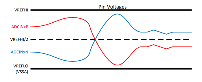
I wanna do a 16 bit read on the MCU. As I can see that, Both ADCINxP and ADCINxN can swing between VREFHI and VSS.
My analogue signal is ranging from0 to 3V and is single-ended. I have connected this signal to ADCINA1 and ADCINA0 is grounded. Now I am using the given example in driverlib for 16 bot mode. I am not able to interpret the results.
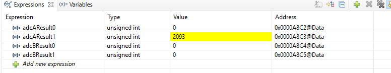
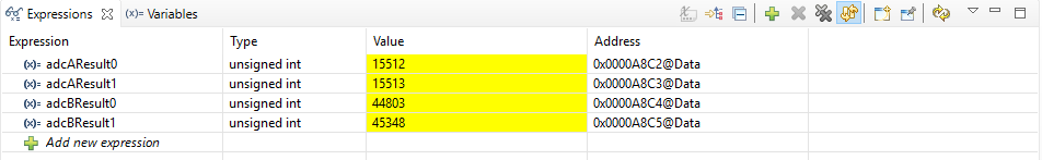
Please find the Captures below. My input signal is 1.5V.
Single Ended.
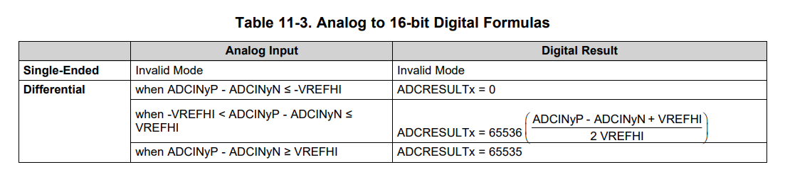
Differential
Whatever I am doing is correct? Do I need any change in the given example for 16-bit mode (other than changing the resolution to 16 bit)? or I need to convert my the signal to differential?
Do I need to add adcAresult0 and adcResult1 in 16-bit mode to get the result?
Comparing above, I am getting the correct value in single-ended mode.
Regards
Vishal Kakade