Part Number: TMS320F28377D
Tool/software: Code Composer Studio
Hi:
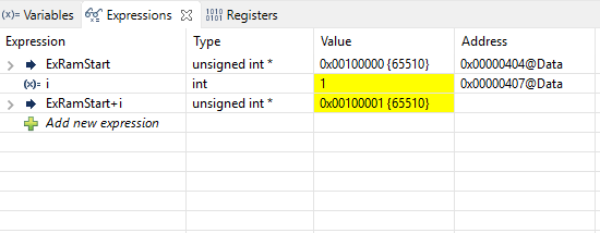
I am trying to get access to addresses from 0x00100000 to 0x00100008, which in the CS2 area. Follow the Technical Reference Manual, EMIF has been configured as the asynchronous mode. For reading/writing 16-bit words, A0 is connected to EMxBA1, [A7: A1] are connected to [A6: A0]. However, form the logical analyzer (Signaltap II), 28377d is not output correct address. CS2 signal kept at 1. RNW at 0. AWE at 1. In addition, the pointer monitored in CCS is correct. It is quite strange.
I attached my code. Could somebody give me a hint? Many Thanks.
#include "F28x_Project.h"

void main(void)
{

	InitSysCtrl();

	EALLOW;
	ClkCfgRegs.PERCLKDIVSEL.bit.EMIF1CLKDIV = 1; // PLLSYSCLK 1/2 for EMIF
	EDIS;

	InitGpio();

	EALLOW;
	//led
	GpioCtrlRegs.GPEMUX1.bit.GPIO133=0;
	GpioCtrlRegs.GPEDIR.bit.GPIO133=1;

	//cs2 rd we
	GpioCtrlRegs.GPBMUX1.bit.GPIO32=2; //cs0	LOW ENABLE
	GpioCtrlRegs.GPBMUX1.bit.GPIO34=2; //cs2	LOW ENABLE
	GpioCtrlRegs.GPBMUX1.bit.GPIO33=2; //RNW	HIGH ENABLE
	GpioCtrlRegs.GPAMUX2.bit.GPIO31=2; //WE		LOW ENABLE
	GpioCtrlRegs.GPBMUX1.bit.GPIO37=2; //EM1OE      LOW ENABLE

	//addr
	GpioCtrlRegs.GPCMUX2.bit.GPIO92=3; 	//EM1BA1
	GpioCtrlRegs.GPBMUX1.bit.GPIO38=2;	//A0
	GpioCtrlRegs.GPBMUX1.bit.GPIO39=2;	//A1
	GpioCtrlRegs.GPBMUX1.bit.GPIO40=2;	//A2
	GpioCtrlRegs.GPBMUX1.bit.GPIO41=2;	//A3

	GpioCtrlRegs.GPBMUX1.bit.GPIO44=2;	//A4
	GpioCtrlRegs.GPBMUX1.bit.GPIO45=2;	//A5
	GpioCtrlRegs.GPBMUX1.bit.GPIO46=2;	//A6
	GpioCtrlRegs.GPBMUX1.bit.GPIO47=2;	//A7

	GpioCtrlRegs.GPBMUX2.bit.GPIO48=2;	//A8
	GpioCtrlRegs.GPBMUX2.bit.GPIO49=2;	//A9
	GpioCtrlRegs.GPBMUX2.bit.GPIO50=2;	//A10
	GpioCtrlRegs.GPBMUX2.bit.GPIO51=2;	//A11
	GpioCtrlRegs.GPBMUX2.bit.GPIO52=2;	//A12

	GpioCtrlRegs.GPCMUX2.bit.GPIO86=2;	//A13
	GpioCtrlRegs.GPCMUX2.bit.GPIO87=2;	//A14
	GpioCtrlRegs.GPCMUX2.bit.GPIO88=2;	//A15
	GpioCtrlRegs.GPCMUX2.bit.GPIO89=2;	//A16
	GpioCtrlRegs.GPCMUX2.bit.GPIO90=2;	//A17
	GpioCtrlRegs.GPCMUX2.bit.GPIO91=2;	//A18
	//GpioCtrlRegs.GPCMUX2.bit.GPIO92=2;	//A19


	//data
	GpioCtrlRegs.GPCMUX1.bit.GPIO69=2;
	GpioCtrlRegs.GPCMUX1.bit.GPIO70=2;
	GpioCtrlRegs.GPCMUX1.bit.GPIO71=2;
	GpioCtrlRegs.GPCMUX1.bit.GPIO72=2;
	GpioCtrlRegs.GPCMUX1.bit.GPIO73=2;
	GpioCtrlRegs.GPCMUX1.bit.GPIO74=2;
	GpioCtrlRegs.GPCMUX1.bit.GPIO75=2;
	GpioCtrlRegs.GPCMUX1.bit.GPIO76=2;
	GpioCtrlRegs.GPCMUX1.bit.GPIO77=2;
	GpioCtrlRegs.GPCMUX1.bit.GPIO78=2;
	GpioCtrlRegs.GPCMUX1.bit.GPIO79=2;
	GpioCtrlRegs.GPCMUX2.bit.GPIO80=2;
	GpioCtrlRegs.GPCMUX2.bit.GPIO81=2;
	GpioCtrlRegs.GPCMUX2.bit.GPIO82=2;
	GpioCtrlRegs.GPCMUX2.bit.GPIO83=2;
	GpioCtrlRegs.GPCMUX2.bit.GPIO85=2;
	EDIS;


	Emif1Regs.ASYNC_CS2_CR.all = (EMIF_ASYNC_ASIZE_16    | 	//16位内存
								  EMIF_ASYNC_TA_4        |
								  EMIF_ASYNC_RHOLD_8     |
								  EMIF_ASYNC_RSTROBE_64  |
								  EMIF_ASYNC_RSETUP_16   |
								  EMIF_ASYNC_WHOLD_8     |
								  EMIF_ASYNC_WSTROBE_64  |
								  EMIF_ASYNC_WSETUP_16   |
								  EMIF_ASYNC_EW_DISABLE  |
								  EMIF_ASYNC_SS_DISABLE);

	DINT;
	InitPieCtrl();
	IER = 0x0000;
	IFR = 0x0000;
	InitPieVectTable();
	EINT;

	int i;
	Uint16 *ExRamStart = (Uint16*)0x00100000;
    for(i=0; i<0x0008; i++)
    	{
          *(ExRamStart+i)=0x6666;
    	}


    while(1)
    {
		GpioDataRegs.GPECLEAR.bit.GPIO133=1;
		DELAY_US (500000);
		GpioDataRegs.GPESET.bit.GPIO133=1;
		DELAY_US (500000);
    }

}