Part Number: TMS320F280049C
Other Parts Discussed in Thread: BOOSTXL-DRV8320RS, EK-TM4C1294XL
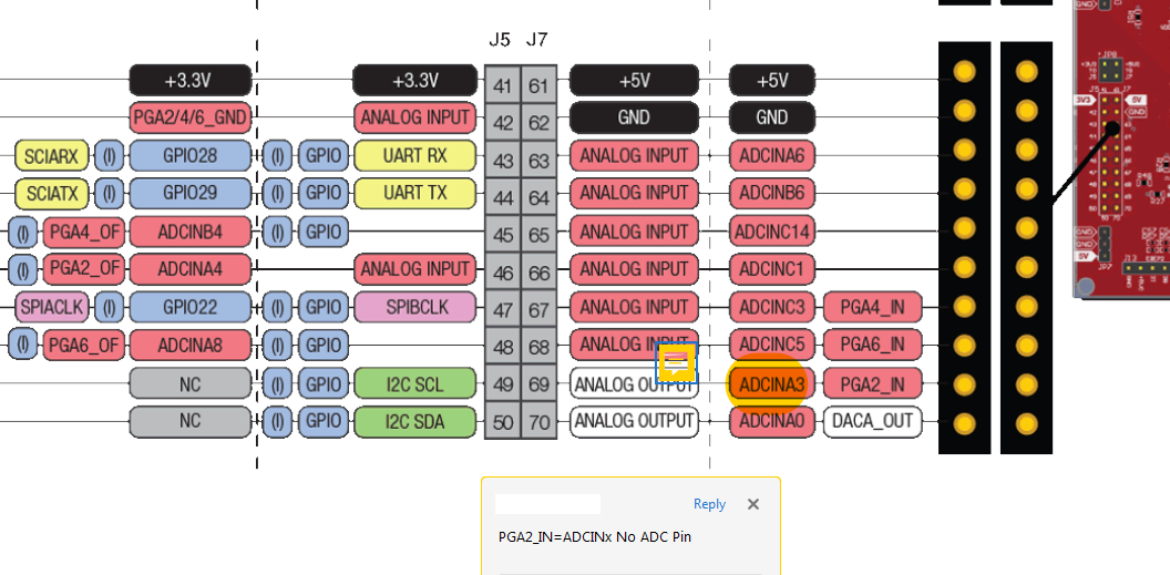
Reviewing the Booster Pack Pin Map card and page 8 of Launch Pad Development Kit SPRUII7A–June 2018–Revised March 2019:
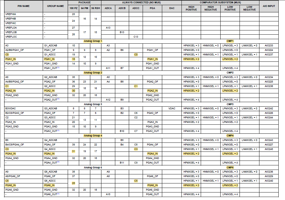
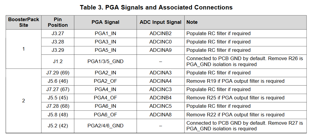
J7 Site2 pin 64 is marked ADCINB6 yet schematic shows pin 64 as ADCINA2. Note pin 64 is voltage sense B for BoostXL-drv8320rs kit site 2 header J7 expects ADCINA2 but SDK expects ADCINB6. I don't find code (hal.c) where the Analog Mux has been configured either B6 or A2 as firmware was commented below. How can pin 64 have 2 ADC's even though base address points to specific ADC and the Analog Subsystem was not configured for shared ADC to disconnect partners from the analog interconnect (TRM Pg.1450 Fig12-1)? Why would the Pin Map card and schematic not show both A2 and B6 if either one can be selected, is that not creating confusion by omitting details?
Perhaps firmware should HWREG command a disconnect any other ADC shared PIN input that is not being used on the analog subsystem, e.g. A2 or B6? The reason to do that seems obvious as to reduce source noise on the analog interconnect from dead ended antenna inputs leading further into the Analog Subsystem. I don't believe setting the ADC base address is going to achieve any necessary isolation of the shared input to other ADC's. It would seem the analog interconnect sub system (Table 12-1) firmware should enable/disable any specific or shared package pin.
Seemingly from the perspective of TI provided detail a conflict has occurred across several documents for the proper identification of pin 64 as to which ADC owns pin 64 (A or B). If one typically expects Pin Map card being reliable, might anyone tend to believe the schematic or both of being incorrect? Some are not so familiar with the multi ADC this MPU has adopted.
    // VSENB - B6/A2->RB1
    ADC_setupSOC(obj->adcHandle[1], ADC_SOC_NUMBER1, ADC_TRIGGER_EPWM1_SOCA,
                 ADC_CH_ADCIN6, HAL_ADC_SAMPLE_WINDOW);

ADCBRESULT_BASE             0x00000B20U // ADCB Result Registers