This thread has been locked.

If you have a related question, please click the "Ask a related question" button in the top right corner. The newly created question will be automatically linked to this question.

TMS320F28069: Is it possible to read multiple ADC(e.g,channel(1,2,5,7)) in single CLA Task

Part Number: TMS320F28069

Hi,

I am working on project in which sensing of various voltages and currents has to be done.

So, I am planning such that,

1)Trigger CLA Task 1 with Rising edge of ePWM1 .

As CLA Task 1 Triggered,

2)Reading all the ADC Channels in that CLA task, and save values in the individual memory for control loop.

So, Is it possible or something else i should follow?

Thank you

Your Faithfully

Mihir Dave

  • Yes, a CLA task can read each of the result registers. 

    Regards

    Lori

  • Hi, 

    So, now as soon as CLA Task 1 is Triggered SOC will be given to first ADC channel(ADC configured in round robin mode) (i.e,1) and after completing conversion of channel 7th ,EOC will be received and CLA Task 1 will send Task completion Interrupt.

    Right ?

    now ,I can Trigger and Read each of the 4 ADC channels during Single CLA TASK 1?

    Thank you

    Your Faithfully

    Mihir Dave

  • I would suggest the scheme discussed in this thread:

    https://e2e.ti.com/support/microcontrollers/c2000/f/171/t/884624

    Regards

    Lori

  • Thank you for the above link it was useful, But still I have one question that can i read multiple ADC at time in CLA ?

    Thank you

    Your Faithfully

    Mihir Dave
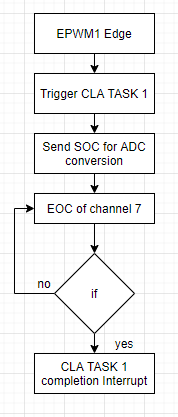
  • If the conversion is complete, then yes, you can.  This will depend on your system. Each task has access to all the peripherals that the CLA can access.  A task is not limited to reading only one ADC.  

    Regards

    Lori

  • //###########################################################################
    // Description:
    //!  \addtogroup f2806x_example_list
    //!  <h1>CLA ADC (cla_adc)</h1>
    //!
    //! In this example ePWM1 is setup to generate a periodic ADC SOC.
    //! Channel ADCINA2 is converted. When the ADC begins conversion,
    //! it will assert ADCINT2 which will start CLA task 2.
    //!
    //! Cla Task2 logs 20 ADCRESULT1 values in a circular buffer.
    //! When Task2 completes an interrupt to the CPU clears the ADCINT2 flag.
    //!
    //! \b Watch \b Variables \n
    //! - VoltageCLA       - Last 20 ADCRESULT1 values
    //! - ConversionCount  - Current result number 
    //! - LoopCount        - Idle loop counter
    //
    //
    //###########################################################################
    // $TI Release: F2806x C/C++ Header Files and Peripheral Examples V151 $
    // $Release Date: February  2, 2016 $
    // $Copyright: Copyright (C) 2011-2016 Texas Instruments Incorporated -
    //             http://www.ti.com/ ALL RIGHTS RESERVED $
    //###########################################################################
    
    #include "DSP28x_Project.h"     // Device Headerfile and Examples Include File
    #include "CLAShared.h"
    #include "string.h"
    
    // Prototype statements for functions found within this file.
    __interrupt void cla1_isr2(void);
    
    // Global variables used in this example:
    #pragma DATA_SECTION(ConversionCount, "Cla1ToCpuMsgRAM");
    #pragma DATA_SECTION(VoltageCLA,      "Cla1ToCpuMsgRAM");
    
    Uint16 ConversionCount;
    Uint16 LoopCount;
    Uint16 VoltageCLA[NUM_DATA_POINTS];
    
    // These are defined by the linker file
    extern Uint16 Cla1funcsLoadStart;
    extern Uint16 Cla1funcsLoadEnd;
    extern Uint16 Cla1funcsRunStart;
    extern Uint16 Cla1funcsLoadSize;
    
    main()
    {
    
    // Step 1. Initialize System Control:
    // PLL, WatchDog, enable Peripheral Clocks
    // This example function is found in the F2806x_SysCtrl.c file.
       InitSysCtrl();
    
    // Step 2. Initialize GPIO:
    // This example function is found in the F2806x_Gpio.c file and
    // illustrates how to set the GPIO to it's default state.
    // InitGpio();  // Skipped for this example
    
    // Step 3. Clear all interrupts and initialize PIE vector table:
    // Disable CPU interrupts
       DINT;
    
    // Initialize the PIE control registers to their default state.
    // The default state is all PIE interrupts disabled and flags
    // are cleared.
    // This function is found in the F2806x_PieCtrl.c file.
       InitPieCtrl();
    
    // Disable CPU interrupts and clear all CPU interrupt flags:
       IER = 0x0000;
       IFR = 0x0000;
    
    // Initialize the PIE vector table with pointers to the shell Interrupt
    // Service Routines (ISR).
    // This will populate the entire table, even if the interrupt
    // is not used in this example.  This is useful for debug purposes.
    // The shell ISR routines are found in F2806x_DefaultIsr.c.
    // This function is found in F2806x_PieVect.c.
       InitPieVectTable();
    
    // Interrupts that are used in this example are re-mapped to
    // ISR functions found within this file.
       EALLOW;  // This is needed to write to EALLOW protected register
       PieVectTable.CLA1_INT2 = &cla1_isr2;   
       EDIS;    // This is needed to disable write to EALLOW protected registers
    
    // Step 4. Initialize all the Device Peripherals:
    // This function is found in F2806x_InitPeripherals.c
    // InitPeripherals(); // Not required for this example
       InitAdc();         // For this example, init the ADC
       AdcOffsetSelfCal();
    
    // Step 5. User specific code, enable interrupts:
    
    // Enable ADCINT1 in PIE
       PieCtrlRegs.PIEIER11.bit.INTx2 = 1;      // Enable INT 11.2 in the PIE (CLA Task2)
       IER |= M_INT11;                          // Enable CPU Interrupt 11
       EINT;          						    // Enable Global interrupt INTM
       ERTM;          						    // Enable Global realtime interrupt DBGM
    
    // Copy CLA code from its load address to CLA program RAM
    //
    // Note: during debug the load and run addresses can be 
    // the same as Code Composer Studio can load the CLA program
    // RAM directly. 
    // 
    // The ClafuncsLoadStart, Cla1funcsLoadSize, and ClafuncsRunStart
    // symbols are created by the linker. 
       memcpy(&Cla1funcsRunStart, &Cla1funcsLoadStart, (Uint32)&Cla1funcsLoadSize);    
    
    // Initialize the CLA registers
       EALLOW;
       Cla1Regs.MVECT2 = (Uint16) (&Cla1Task2 - &Cla1Prog_Start)*sizeof(Uint32);
       Cla1Regs.MVECT8 = (Uint16) (&Cla1Task8 - &Cla1Prog_Start)*sizeof(Uint32);
       Cla1Regs.MPISRCSEL1.bit.PERINT2SEL = CLA_INT2_ADCINT2; // ADCINT2 starts Task 2
       Cla1Regs.MMEMCFG.bit.PROGE = 1;          // Map CLA program memory to the CLA
       Cla1Regs.MCTL.bit.IACKE = 1;             // Enable IACK to start tasks via software
       Cla1Regs.MIER.all = (M_INT8 | M_INT2);   // Enable Task 8 and Task 2
       Cla1ForceTask8andWait();                 // Force CLA task 8.  
                                                // This will initialize ConversionCount to zero
    
       AdcRegs.ADCCTL2.bit.ADCNONOVERLAP = 1;	// Enable non-overlap mode
       AdcRegs.ADCCTL1.bit.INTPULSEPOS = 0;	    // ADCINT trips when ADC begins conversion
       AdcRegs.INTSEL1N2.bit.INT2E     = 1;	    // Enable ADCINT2
       AdcRegs.INTSEL1N2.bit.INT2CONT  = 0;	    // Disable ADCINT2 Continuous mode
       AdcRegs.INTSEL1N2.bit.INT2SEL   = 1;	    // setup EOC1 to trigger ADCINT2 to fire
       AdcRegs.ADCSOC1CTL.bit.CHSEL    = 2;	    // set SOC1 channel select to ADCINA2
       AdcRegs.ADCSOC1CTL.bit.TRIGSEL  = 5;     // set SOC1 start trigger on EPWM1A
       AdcRegs.ADCSOC1CTL.bit.ACQPS    = 6;	    // set SOC1 S/H Window to 7 ADC Clock Cycles, (6 ACQPS plus 1)
       EDIS;
    
    // Assumes ePWM1 clock is already enabled in InitSysCtrl();
       EALLOW;
       SysCtrlRegs.PCLKCR0.bit.TBCLKSYNC = 0;
       EDIS;
       EPwm1Regs.ETSEL.bit.SOCAEN	= 1;		// Enable SOC on A group
       EPwm1Regs.ETSEL.bit.SOCASEL	= 4;		// Select SOC from from CPMA on upcount
       EPwm1Regs.ETPS.bit.SOCAPRD 	= 1;		// Generate pulse on 1st event
       EPwm1Regs.CMPA.half.CMPA 	= 0x0080;	// Set compare A value
       EPwm1Regs.TBPRD 				= 0xFFFF;	// Set period for ePWM1 - this will determine the sampling frequency
       EPwm1Regs.TBCTL.bit.CTRMODE 	= 0;		// count up and start
       EALLOW;
       SysCtrlRegs.PCLKCR0.bit.TBCLKSYNC = 1;
       EDIS;
       
       
    // Wait for ADC interrupt
       for(;;)
       {
          LoopCount++;
       }
    
    }
    
    // This interrupt occurs when CLA Task 2 completes
    __interrupt void cla1_isr2()
    {
        AdcRegs.ADCINTFLGCLR.bit.ADCINT2 = 1;    // Clear ADCINT2 flag reinitialize for next SOC
        PieCtrlRegs.PIEACK.all = 0xFFFF;
    }


    Thanks I will try this,

    Also I have one more doubt,

    As I am taking below program as a reference ,

    there are two variable defined and linked between CLA and CPU

    1)Conversion count 

    2)Voltage CLA 

    So, is it possible to declare and share more than 2 variables between CPU and CLA?

    for e.g; Voltage1,voltage2,current 1,current 2,count 1,count 2.

    Thank you

    Your Faithfully

    Mihir Dave 

  • mihir dave said:

    So, is it possible to declare and share more than 2 variables between CPU and CLA?

    for e.g; Voltage1,voltage2,current 1,current 2,count 1,count 2.

    Yes, please refer to this FAQ: https://e2e.ti.com/support/microcontrollers/c2000/f/171/t/795553

    The CLA hands-on-workshop is very good at describing the CLA, how to develop code for it, and also how to debug it in Code Composer Studio. I think you will find it helpful. Here is the link to the workshop:

    Click here for more CLA FAQs and resources.

    I hope this helps. If this answers your question, please click the green "Verified Answer" button.

  • Thank you Very much