This thread has been locked.

If you have a related question, please click the "Ask a related question" button in the top right corner. The newly created question will be automatically linked to this question.

PGA +IN bias

Guru 56143 points
Part Number: LAUNCHXL-F280049C
Other Parts Discussed in Thread: INA240, BOOSTXL-DRV8320RS

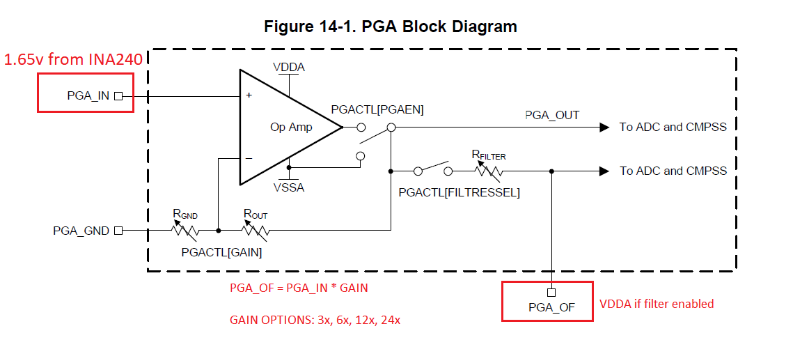
Having enabled PGA resistor filters C32,33,34, removing R19, R22, R25 and set +1.65v bias J7 pins 67,68,69 the OUT signal of each PGA2,4,6 is zero crossing, J5 pins 45,46,48 were disconnected. Consequently the CMPSSx are expecting mid supply +1.65v signal randomly trip ePWM combinational TripIN.  Adding to thread R27 was removed from PGA_GND (-IN) to make it an analog buffer centered 1.65v. And PGA (Rgnd) resistor was not connected but later reconnected via R27 0R. 

1. Why do the PGA outputs not have a threshold set to mid supply after enabling the 3 filters?

2. Is there other configuration required to set mid supply (+1.65v) on the PGA outputs?

Oddly if we use INA240 mid supply (+1.65v) outputs for ADC inputs and bypass disable PGA's the CMPSSx DC filters seem to exhibit a mid supply perspective randomly tripping ePWM faults. The PGA x12 gain do not have this issue so it makes it seem PGA_OUT has <1.65v center.

Note: Analog sub system CMPSSx_LP0/HP0, (TRM Fig12.4).

    // For Motor_1/Motor_2
    for(cnt = 0; cnt < 3; cnt++)
    {
        // Set a gain of 12 to Site1=PGA1/3/5 or Site2=PGA4/6/2
        PGA_setGain(obj->pgaHandle[cnt], PGA_GAIN_3); //12

        // No filter resistor for output
        /* Enable LowPass filter Internal Resistor value for
         * external capacitors C32,33,34, Remove R19,22,25 */
        PGA_setFilterResistor(obj->pgaHandle[cnt],
				  PGA_LOW_PASS_FILTER_RESISTOR_100_OHM); 

        // Enable  Site1=PGA1/3/5 or Site2=PGA4/6/2
        PGA_enable(obj->pgaHandle[cnt]);
    }

  • Hi Gl,

    I'm sorry I'm not clear on your question. The PGA filters have no effect on the DC gain. What input are you supplying to the PGA?

  • The question was very clearly laid out, +IN = +1.65v mid supply either by external DAC pin or by the INA240 set at mid supply.

    The problem seems to be the PGA outputs zero crossing signals into the ADC (Not mid supply), probe J5 output filter pins. Those pins are the output of the PGA amplifiers.

    Why would the PGA output not have a threshold of mid supply if +IN pin has +1.65v bias? The CMPSSx were configured assuming mid supply threshold from PGA outputs. Otherwise it would not have been necessary to invert the low DAC output! Seemingly the reason LOW side inversion got through QC debug check is the value was always below 2048 count being PGA outputs were zero crossing! This seems to explain why the INA240 fails to produce same ID motor results as PGA's configured in the SDK FOC setup. If this indeed is true it must be corrected ASAP to protect the community from such a pandemic!

    Below code was configured incorrectly in the SDK and does not do but 1 function, output CMPSSx CTRIP-H/L into ePWM xBAR via MUX for TripINx. The other two defines do not belong in this function call.

            // Configure the output signals. Both CTRIPH and CTRIPOUTH will be fed
            // by the asynchronous comparator output. 
            CMPSS_configOutputsHigh(obj->cmpssHandle[cnt], CMPSS_TRIP_FILTER |
                                    CMPSS_TRIPOUT_FILTER |
                                    CMPSS_OR_ASYNC_OUT_W_FILT);
    
            CMPSS_configOutputsLow(obj->cmpssHandle[cnt], CMPSS_TRIP_FILTER |
                                   CMPSS_TRIPOUT_FILTER |
    							   CMPSS_INV_INVERTED); 

  • Frank Ankapong said:
    I'm sorry I'm not clear on your question.

    You skirted both question rather than answer points 1 or 2.

  • I'm still not 100% clear on the question you are asking but I'll try and answer it based on my current understanding.

    The PGA does not support voltage follower mode. The minimum gain is 3x so I'm not exactly sure why you expect 1.65v output with a 1.65v input. If you input 1.65v to the PGA, any of the gain settings will cause the output to rail to VDDA.

    The maximum input you can apply to the PGA depends on the gain setting which I list out in the formulas below:

    i. If linearity is important, Max PGA Input = (VDDA - 0.35v)/PGA_GAIN

    ii. If linearity is not important, Max PGA Input = VDDA/PGA_GAIN

    To answer your questions directly:

    1. As i said in the prior response, whether or not you use the PGA filters has no effect on the DC gain. Enabling the PGA filters doesn't suddenly make the PGA a voltage follower.

    2. See above. If you want 1.65v on the output, you will need to input 1.65v/PGA_GAIN

    If I'm still not answering your question, please point out what I'm missing and I'll do my best to answer.

  • Frank Ankapong said:
    The PGA does not support voltage follower mode. The minimum gain is 3x so I'm not exactly sure why you expect 1.65v output with a 1.65v input. If you input 1.65v to the PGA, any of the gain settings will cause the output to rail to VDDA.

    It don't matter what gain has been set 3,6,12,24 the resistor filter output pins remain at VREFLO VDDA. The analog signal is then zero crossing into ADC analog subsystem, TRM 12-1. The SDK software CCMP's assumed PGA outputs were set to mid supply (1.65v) as anyone would assume for use in current scale factors of motor phase current calibration as outlined in SPRUHJ1H–January 2013–Revised June 2019.

    Alternatively the INA240 can be set to unidirectional output (0v-3v3) and using the PGA as a near unity gain (buffer x3). That did not produce usable results with or without PGA input buffers. The PGA has to be useful as in 1:1 analog input buffer for the ADC impedance matching of analog signal sources. PGA are useless for motor control ADC impedance matching of mid supply signals and HV transients can club MCU via very limited input filter BoostXL kit demonstrates. The INA240 has built in transient suppression and PWM rejection which PGA's do not posses. The INA240 demonstrates industry accepted ADC bidirectional current monitor technique via 1.65v mid supply outputs into the ADC channels also accepted by TI engineers several TIDA kits. 

    Otherwise the SDK software would be useless to build upon production systems that don't use PGA inputs for phase current detection. I don't think that is the mission statement for TI launch pads and booster pack development kits. Industry wide matching ADC amps are used to buffer outside analog signals as they exist! 

    Frank Ankapong said:
    2. See above. If you want 1.65v on the output, you will need to input 1.65v/PGA_GAIN

    The PGA output results are in direct conflict with SPRUHJ1H–January 2013–Revised June 2019 documentation.

    Seemingly you are missing the point PGA +IN pin is biased +1.65v via INA240 bidirectional output threshold but the PGA output filter pin remains at VDDA VREFLO when it should be at mid supply (1.65v) due to +IN bias 1.65v. The BoostXL-DRV8320rs using external DAC to bias the +IN of PGA (1.65v) distorts the mV/A calculation and PGA gain levels relative to the selected low side shunt resistive value. The INA240 is not working correctly with SDK scale factor and ADC formula where the PGA outputs should have +1.65v center to begin with. There is no documentation that discusses SDK has made this incompatible current monitor change.

    //! \brief Defines the maximum current at the AD converter
    //! BOARD_BSXL8320RS_REVA Gain=12, INA240 Gain=20
    #define USER_ADC_FULL_SCALE_CURRENT_A

    Again this PGA issue is far outside any TI documentation via SPRUHJ1H–January 2013–Revised June 2019.

    The result is the SDK scale factor ADC formula only works for the BoostXL-DRV8320Rs and produces incorrect motor ID calculations via custom DC inverter hardware. Seemingly odd PGA_OUT behavior was due to R26/R27 0R to ground on the PGA inverting inputs

  • Frank Ankapong said:
    If you input 1.65v to the PGA, any of the gain settings will cause the output to rail to VDDA

    Note the (red) corrections above post meant to type VREFLO not VDDA. That is not occurring as the output rails to VREFLO but if we touch the filter pin JP5 - 45,45,48 with +1.65v +IN bias the 60Hz signal is zero crossing. That seems to infer the PGA incorrectly outputs zero crossing signals into the analog subsytem and ADC channels. 

    Again the CCMPS low side inverted output configuration relative to using 2048 ADC counts to trigger ePWM TripIN is a clue engineer expected the PGA output to be at mid supply. That is my perspective too and it seems to work with INA240 but not the PGA or Rfilter output pins siting at VREFLO.

    Perhaps driver lib call to configure Rfiler is not asserting selected values since the output remains VREFLO?  

  • Gl,

    There seems to be a big miscommunication going on. I'll try to explain it again with the aid of a diagram.

    The PGA on the F280049 device is hard-coded in a non-inverting amplifier configuration, you can't change this. Unity gain mode or voltage follower mode is not supported.

    Looking at the figure above from the TRM, can you help me understand why exactly you think a 1.65v on PGA_IN should result in 1.65v on PGA_OF?

    To answer your second question: If you are seeing 0v on PGA_OF, it means no supported filter option is enabled. You can look at the FILTRESSEL field of the PGACTL register in the watch window. You should see a number between 1 to 6.

  • Frank Ankapong said:
    an you help me understand why exactly you think a 1.65v on PGA_IN should result in 1.65v on PGA_OF?

    PGA_IN is biased to 1.65v so  PGAEN output must center near 1.65v, not VREFLO as shows up on PGA_OF when FILTRESSEL was configured. No other way to verify the PGA_OUT is actually centered on 1.65v via DMM or scope probe, PGA_GND = R27 removed. That 1.65v center was the typical way motor driver kits monitor low side shunt current of past control suite and other TIDA kits. Point being the PGA_OUT has to swing more than +/-500mV in either direction for the ADC to scale higher phase currents with any precision via 1.65v center to VDDA and 165v down to VREFLO. I realize the PGA is not true rail to rail 350mV loss and the INA240 rails roughly 200mV < 3v3.

    The point is the SDK should work well with INA240A1 x20 gain without PGA but fails to produce correct ADC results. The SDK was tweaked for PGA behavior to control FAST estimator and seemingly will not produce correct LC inductance without duplicating the same filter of the BoostXLDRV-8320rs. So I added 2200pf caps for the PGA's external filters, set 100 ohm Rfilter and the voltage was not centered 1.65v as expected. Hence the INA240 was using the PGA as the ADC input buffer it was also to be used for. The PGA_OUT was centered on REFLO according to the results on the filter output pins. The INA240 forum gurus will argue center 1.65v output for ADC is the holy grail for bipolar current detection.

    See SPRUHJ1H–January 2013–Revised June 2019 Page 356 Fig. 8-11, 8-12

    Why use the PGAs when external amplifiers are already being used? One case would be if many different current rated motors are powered with the same inverter. Amplification of the current signal can be adjusted to best suit the motor size that is controlled. The output of the PGA block is the input of the comparator windows. The PGA still needs to be connected to enable the use of the fault detection circuitry. Not so true of x49c MCU.

  • I may have forgotten to add the PGA_GND (-IN) was not tied to VREF_LO and R27 was removed. So the PGA should behave as a buffer stage into the ADC and PGA_OUT center near 1.65v as the inverting input has PGA_OUT feed back hysteresis to offset phase margin at 20kHz.

    Have a look at page 230 Fig. 5-4 is more close to what I was attempting with the PGA as buffer stage for INA240.

  • Perhaps the problem is R27 0R needs to be 1k or greater to allow the PGA_OUT to swing +/-1.65v. That I have not yet tested but the ADC scale factor was set 76A FS for the INA240 2mohm shunt value 40mV/A. I'm not sure if the User_ADC_SF will even work for 80A detection as SDK seemed to almost work with 40A SF. At least Motor ID lab5 50Hz speed got further into RatedFluxOL time wait prior to tripping PWM fault. Otherwise the SDK BoostXL-DRV8320rs motor ID'd a stalled 20Hz rotor for having the correct inductance was simply wacko but oddly it worked!  


  • Upgraded 2mohm shunts to 5mohm and reduced the USER_ADC_FULL_SCALE_CURRENT_A =(32.7) and IA_OFFSET_A/B/C=(-16.35). The same issue occurs INA240 mid supply trips CMPSSx DC comparators ePWM TripIN upon entering EST_STATE_RATEDFLUX_OL. The higher 5 millivolt shunt would drive the input of differential amp much harder than 2mv. 

  • Frank Ankapong said:
    2. See above. If you want 1.65v on the output, you will need to input 1.65v/PGA_GAIN

    Did you really mean to say the PGA output will center 1.65v if the PGA_IN bias is divided by the PGA_GAIN?

    So input bias 1.65v / x12 = output center of 0.55V? The first part of your statement contradicts the second part formula.  

    Should get 1.65v Vadcin center for x3 gain according to Fig.8-12, AFE formula above post for several other listed C2000. 

    Judging from how  CMPSS DAC filters are tripping ePWM faults (Vadcin 1.65) it appears the PGA_OUT was centered more like 0.55v.


  • The boostxl-drv8320rs PGA_OUT's I have confirmed to be centered 1.68v via the PGA filter outputs scope J5 - pin 45,46, 48 first removing the 300pF caps.

    Have confirm the user FS was oddly set 42A seemingly is not possible via 140mV/A input bias using the potentiometer rule to work the filter math. The best ADC 1/2 scale PTP current from 7mohm shunt (x12) gain is little less than 20 amps. Measured from ADC 2048 counts up to VDDA and from perfect 0 (1.68v) down to -2048 VSSA (0v).

    I noticed an immediate difference from the INA240 on our DC inverter amps to that of BoostXL current detection PGA amps. It seems the ADC current scale factor was set twice as high as the actual mV/A from filter. Without CMPSS to manage OVC DC trips there is only the boostXL Tz2 output to trip at peak current as configured. Obviously the SDK (FOC) did not have the DC source configured for ePWM trips, perhaps this was a WA to get NexFET peak 40A output but in some off hand obscure way. Otherwise the CMPSS DCA/B sources did not trip ePWM faults as they now do after adding in DC sources for Trip zone actions. 

    The input filter math: Vin * (R2/R1+R2) = 0.14028286141788452797730261667273 PGA_IN bias x 12 = 1.68v center PGA_OUT.

    User ADC full scale set to perfect 0v 2048 counts: 1.68v / 0.140mV/A = 24A Peak not 42A. The 7mohm shunt (7mv/A) was factored out via PGA_IN bias x12 gain. Seemingly the best way to increase ADC +/- half scale (2048) counts is to reduce the shunt value from 7mohm to 3mohm to derive a 42A Peak FS? Seemingly the kit was limited to 24A peak when Boostxl-drv8320rs claims 40A peak drive current. This seems to explain why >10µH stator inductance rotor stalls at 20Hz when it should not. 

    Perhaps the SDK developers noticed this odd issue and further restricted the ADC 24A Peak?

    //! \brief Defines the maximum current at the AD converter
    //!        BOARD_BSXL8320RS_REVA Gain=12 140mV/A, INA240 Gain=20 40mV/A
    #define USER_ADC_FULL_SCALE_CURRENT_A         ((float32_t)(42.843))


  • I forwarded this question on to the developer for that software. Their response was that information in the thread was unclear and we would need a schematic to clarify what your system is, which will help them to understand and attempt to answer your question.

    Regards,
    Cody  

  • The values 2048 had really confused me, HAL had set DC comparator filter to mid supply 2048 but it was not working to trip ePWM faults. Until I found the DC filter settings were being overwritten later inside lab5 using completely different filter values than HAL had initialized. No one would even look for such an over write and defeats the intention of the HAL in my mind. Later after this post stumbled into the bees nest to find the other DC values were just as wrong.

    The point was in last post the Peak current set as ADC full scale seems wrong as perfect zero divides 4096/2 for +/- integers ADC samples of bidirectional phase current 40A PTP, not 20A PTP. Each SVPWM sector Uout  has 2 possibilities based on sample values _IA_,  _IV_ used to determine rotation angles via FAST estimator. 

    The PGA2,4,6_OF were actually centered 1.68v but the DCA/B L/H filter value 2048 was set to perfect 0 (1.68v center), not the ePWM trip point as configured via the HAL. Seemingly 7mohm shunt restricts PTP phase current +/-20A in CMPSS DCA/B. Yet NexFET datasheet shows 40Arms winding current, 400A single pulse <100µs. RMS winding current = 0.707*Peak. PGA_OUT samples are not RMS and ADC FS value perhaps should be twice PTP value. Seemingly should be 2*ADCFS /2*0.707 to allow 40Arms peak via the NexFETS.

    Otherwise rotation angles acquired via FAST estimator may cause rotor vibration as occurs consistently in smaller rotors after motor ID=true. Short of it (1/2 FS=2048 40A PTP ) seemingly not ADC FS 40A Peak as each 1/2 cycle of winding current occurs 180° out of phase in a perfect 360° circle. Neither half of the current (A) sine wave or power (W) occur at the same time in the sample rate. Only one 1/2 cycle is captured each 50µs period at 20Khz PWM. At least the INA240 idea of precision our custom inverter 80A FS window, the LtoL RS ohms value is much easier to achieve with higher FS Amps. In the context of current measure how does NextFET datasheet claim Iout=40Arms stack up to/with the SDK sample of PTP RMS current with 7mohm shunt?