This thread has been locked.

If you have a related question, please click the "Ask a related question" button in the top right corner. The newly created question will be automatically linked to this question.

DCL A/B fails to clear latches

Guru 56198 points

Part Number: LAUNCHXL-F280049C
Other Parts Discussed in Thread: BOOSTXL-DRV8320RS

If we don't configure combinational DCA/B for Low TripINx for ePWM xBAR MUX H or L, the Low DAC digital filters remain latched after SW clears them.

If we do configure combinational DCA/B for both low/high state/path of TripINx events then SW clears Low side latches, otherwise low remain latched.

Yet the ePWM digital compare event condition is set for High state. So the low DC state should be cleared upon CPU reset and ignored but trips immediate faults upon SW reading fault now flag bits. 

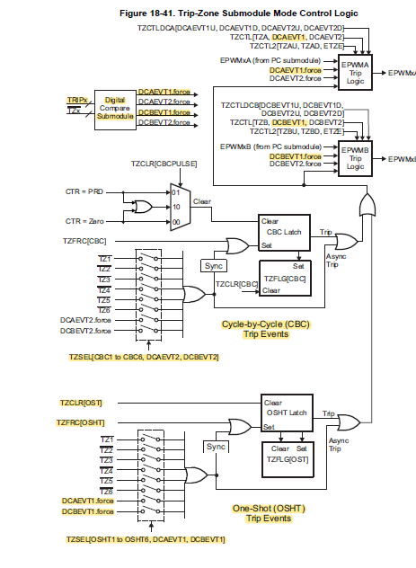
1. Why is it any better if not even counter productive to have both DC H/L states/path trip PWM faults even after trip sub module is configured for High trip events only? 

2. Why was the CMPSSx ASYNCH DC path and the digital filter both configured in the SDK along with Output xBAR as a conflicting configuration?

3. Seemingly It is not even possible to configure an Or'd asynch latch on the ASYNCH (0) path and expect the digital filter to work (TRM Fig.16-1) but we only need CTRIPH/L unlatched events.

4. There is no ASYNCH path for the DC filter depicted (Fig.16-1) and CMPSS_OR_ASYNC_OUT_W_FILT define is oddly missing or it is it path (3)?

5. Why was CTRIPOUTH/L originally configured as they both go to the Output xBAR and are a dead end path.

Note too the DC output inversion was set on the wrong call in the SDK (corrected below). That may not have done any harm but the DC filter sample clock ticks are being ignored, seemingly odd errata passes all counts >2048 as false trips.  

 Patched snips:

        /* Configure inverting input for internal COMPDAC(VDDA3v3) reference
         * and low comparator inverted both with non-asynch filter outputs  */
        CMPSS_configHighComparator(obj->cmpssHandle[cnt],
					CMPSS_INSRC_DAC );   // CMPSS_OR_ASYNC_OUT_W_FILT
        CMPSS_configLowComparator(obj->cmpssHandle[cnt],
					CMPSS_INSRC_DAC | CMPSS_INV_INVERTED);

        // Configure digital filter. For this example, maximum sense values
        // were used for the clock prescale, sample window size,
        // Prescale: clock ticks between samples <1024, Sample window: Not >32,
        // threshold: < Sample window/2 but 1< than filter threshold
        CMPSS_configFilterHigh(obj->cmpssHandle[cnt], 256, 3, 2);//4,3,2
        CMPSS_configFilterLow(obj->cmpssHandle[cnt], 256, 3, 2);

        // Configure the output signals. CTRIPH but NOT CTRIPOUTH will be fed
        // by asynchronous comparator output and only CTRIPH MUX's into ePWM xBAR
        CMPSS_configOutputsHigh(obj->cmpssHandle[cnt], CMPSS_TRIP_FILTER); //CMPSS_TRIP_LATCH
        //
        CMPSS_configOutputsLow(obj->cmpssHandle[cnt], CMPSS_TRIP_FILTER); //CMPSS_TRIP_LATCH

        // SW clear high comparator digital filter output latch
        CMPSS_clearFilterLatchHigh(obj->cmpssHandle[cnt]);

        // SW clear low comparator digital filter output latch
        CMPSS_clearFilterLatchLow(obj->cmpssHandle[cnt]);

// Rem code below holds CMPSTSn status latched even after SW clear

        // DC TRIP combinational inputs
        // 18.11.12 CMPSS: EPWM_DC_COMBINATIONAL_TRIPIN2 (GPIO)
        // From CCMPSSx DC A/B CTRIP-H/L
        // TRM Pg.1872 Fig.18-48
        /* Combinational DCA into PWM-A1 */
        EPWM_enableDigitalCompareTripCombinationInput(obj->pwmHandle[cnt],
               (EPWM_DC_COMBINATIONAL_TRIPIN5 |
                EPWM_DC_COMBINATIONAL_TRIPIN7 | EPWM_DC_COMBINATIONAL_TRIPIN9),
                EPWM_DC_TYPE_DCAH);
        //EPWM_enableDigitalCompareTripCombinationInput(obj->pwmHandle[cnt],
               //(EPWM_DC_COMBINATIONAL_TRIPIN5 |
		//EPWM_DC_COMBINATIONAL_TRIPIN7 | EPWM_DC_COMBINATIONAL_TRIPIN9),
                //EPWM_DC_TYPE_DCAL); 
        /* Combinational DCB into PWM-B1 */
        EPWM_enableDigitalCompareTripCombinationInput(obj->pwmHandle[cnt],
               (EPWM_DC_COMBINATIONAL_TRIPIN5 |
                EPWM_DC_COMBINATIONAL_TRIPIN7 | EPWM_DC_COMBINATIONAL_TRIPIN9),
                EPWM_DC_TYPE_DCBH); 
        //EPWM_enableDigitalCompareTripCombinationInput(obj->pwmHandle[cnt],
               //(EPWM_DC_COMBINATIONAL_TRIPIN5 |
                //EPWM_DC_COMBINATIONAL_TRIPIN7 | EPWM_DC_COMBINATIONAL_TRIPIN9), 
                //EPWM_DC_TYPE_DCBL); 

        // Trigger event when DCAH is High
        EPWM_setTripZoneDigitalCompareEventCondition(obj->pwmHandle[cnt],
                                                     EPWM_TZ_DC_OUTPUT_A1,
                                                     EPWM_TZ_EVENT_DCXH_HIGH);

        // Trigger event when DCAL is High
        EPWM_setTripZoneDigitalCompareEventCondition(obj->pwmHandle[cnt],
                                                     EPWM_TZ_DC_OUTPUT_B1,
                                                     EPWM_TZ_EVENT_DCXL_HIGH);

  • Oddly if we set MUXn point to port 1 for DAC trip High the low side DCA latches still remain set after SW clear. One has to question this code below as it leads to the combinational TripIN. REM'd out both A/B low ePWM combo (above post) seemingly are CBC trip events? Only the OSHT xBAR events are left to trip ePWM TripINx faults?

    The define seems oddly to claim a DCH/L Boolean (State) event rather than DCH/L (Path) to the ePWM xBAR and combinational TripINx configured above post.

    Refer TRM: Fig.18-41 page 1865 Trip-zone submodule Control Logic.

    1. Is below MUX define Path or Bool State as name is very confusing how H/L DAC path or state translates into a ePWM xBAR, OSHT or CBC path?

        // TRM:9.2.1 Table 9-2
        // Configure TRIP5 to be CTRIP2H and CTRIP2L via ePWM xBAR PWM A/B
        XBAR_setEPWMMuxConfig(XBAR_TRIP5, XBAR_EPWM_MUX02_CMPSS2_CTRIPH_OR_L);
        XBAR_enableEPWMMux(XBAR_TRIP5, XBAR_MUX02);
    
    //State or Path: XBAR_EPWM_MUX02_CMPSS2_CTRIPH?
          //Ditto XBAR_EPWM_MUX02_CMPSS2_CTRIPH_OR_L?

  • It seems odd contention CMPSSx DAC CTRIPH/L outputs are event paths (DCAEVNT1 / DCBEVENT2) Fig.18-41 and named EPWM_DC_TYPE_DCAH/BL. Both events 1A/1B(OSHT) or 2A/2B(CBC) are DAC events sent to ePWM trip-zone submodule Mode control and the defined combinational trip zones in DC high level sub module Fig.18-48.

    Yet how does the name not being configured for CBC (combinational) events cause CMPSS DCB low latches to remain latched?

    The CBC/OSHT DCA/B events are configured via EPWM_setDigitalCompareEventSource() and EPWM_setTripZoneDigitalCompareEventCondition for OSHT combinational events A1/A2. B1/B2 CBC combinational events should have nothing to do with DCB latch or status events sources since they were not configured.

    Perhaps a less confusing define name for each DAC sub module combinational event (DCAEVNT1_OSHT and DCBEVNT2_CBC). This way the TRM names align with driver lib defines!

  • Anyone know how or see the mistake in first posted code and or what that has to do with SW clearing COMPLLATCH, CMPLSTS per Fig. 18-41? 

    Hint: The original SDK code was configured for both CBC/OSHT CMPSSx DCA/B events but neither one actually cleared CMPSSx latch flags. SW clear Filter latch fails to clear the latch flags!

            // SW clear high comparator digital filter output latch
            CMPSS_clearFilterLatchHigh(obj->cmpssHandle[cnt]);
    
            // SW clear low comparator digital filter output latch
            CMPSS_clearFilterLatchLow(obj->cmpssHandle[cnt]);

    That said it would seem there was no actual combinational CMPSSx events being passed and fault protection only via Tz2 - if it indeed worked. We never witnessed a single time BoostXL-drv8320rs tripped faults LED but it did burn two Nidec motors via lab5 motor ID. 

  • Which SDK are you using?

    EPWM XBAR outputs (TRIPIN1-x) is not related to H/L DC. TRIPINx are related to TZx inputs.

    DCAEVT1 and DCBEVT1 are used for OSHT

    DCAEVT2 and DCBEVT2 are used for CBC

    But DCAEVT1/DCAEVT2 and DCBEVT1/DCBEVT2 can be sourced from the TRIPINx inputs.

    I have notified Frank our CMPSS expert as well.

  • Hi Nima,

    Nima Eskandari said:
    Which SDK are you using?

    FOC SDK and you did't find the REM mistake above that somehow leads to DAC low latch not being cleared. Either combinational A1/2 or B1/2 not being configured should not effect the CCMPSSx latches but does. There was definitely path issues in the CCMPSSx DAC configurations. This gating has to be so spread apart for TRM discussion so it becomes difficult to put it all together and naming conventions count 100%. 

    The original SDK code had both CBC and OSHT combinational but had no source or action, can't recall which one or both. Since Tz2 is not being used in this config, I stuck DACA1/B1 events as TzActions and removed the advance action counter compare parts to KISS it up. Saddy EPWM_setTripZoneAction() would not let me OR EPWM_TZ_ACTION_EVENT_TZA/B with DCA1/B1, it's one or the other. That is why we are being forced to add advance TZ actions just for DCA1/B1 and or DCA2/B2 when Tz2 is also used.


  • Gl said:
    That is why we are being forced to add advance TZ actions just for DCA1/B1 and or DCA2/B2 when Tz2 is also used.

    Not being forced but that was the only option since CCS code analysis complained there were conspicuous passed entries "Enumerated type mixed with another". Find it odd that there are only advance PWM counter compare Tz actions for CMPSSx DCA/B. That is if anyone chooses Tz2 and then no other TripINx are allowed to be OR'd. That seems counter intuitive to how the Tz sub module shows multiple TripINx besides the combinational inputs.

    EPWM_setTripZoneAction() allowed DCA1/B1 events but denied any others as passed entries via CCS code analysis. How is the function assert correct to deny but 1 event entry for the Tz sub module action? Seemingly CCS code analysis error is barking up the wrong tree?

  • Nima Eskandari said:
    I have notified Frank our CMPSS expert as well.

    Good point as the combinational TripINx are neither High or Low - they are inputs into the DC submodule (Fig.18-41) multi OR gate stage or DC trip select ports Fig.18-48. How are DCA/B both bool state and DCA/B events into the combinational multi OR gate.   The logic of OR gate any input High so the compare Low state does not exist and there is no compare combinational function. The select OR event only closes the switch for the OR gate for High states from DCA/B to pass and the low state does nothing. That is unless the OR gate has Tz sub module state control logic but that was not depicted Fig.18-48 and it obviously matters some how some way, according to driver lib defines.

    These defines are what is confusing me perhaps should be OSHT or CBC events driven by Fig.18-41. The MUX config table 18-13 selects trip event H/L and DCA/B_H or L but seems to infer either position of CMPSS DAC, not a Bool state. The signal state is determined by the action qualifier for the Digital compare event conditions show below. 

    //!      - EPWM_DC_TYPE_DCAH  - Digital Compare A High
    //!      - EPWM_DC_TYPE_DCAL  - Digital Compare A Low
    //!      - EPWM_DC_TYPE_DCBH  - Digital Compare B High
    //!      - EPWM_DC_TYPE_DCBL  - Digital Compare B Low
    //!
            // Trigger event when DCAH is High
            EPWM_setTripZoneDigitalCompareEventCondition(obj->pwmHandle[cnt],
                                                         EPWM_TZ_DC_OUTPUT_A1,
                                                         EPWM_TZ_EVENT_DCXH_HIGH);
    
            // Trigger event when DCAL is High
            EPWM_setTripZoneDigitalCompareEventCondition(obj->pwmHandle[cnt],
                                                         EPWM_TZ_DC_OUTPUT_B1,
                                                         EPWM_TZ_EVENT_DCXL_HIGH);
    
    
            // Configure the DCA path to be un-filtered
            // Unfiltered: EPWM_DC_EVENT_SOURCE_ORIG_SIGNAL
            // Blanking filter: EPWM_DC_EVENT_SOURCE_FILT_SIGNAL
            EPWM_setDigitalCompareEventSource(obj->pwmHandle[cnt],
                                              EPWM_DC_MODULE_A,
                                             EPWM_DC_EVENT_1,
    			  EPWM_DC_EVENT_SOURCE_ORIG_SIGNAL);
    
            // Configure the DCB path to be un-filtered
            EPWM_setDigitalCompareEventSource(obj->pwmHandle[cnt],
                                              EPWM_DC_MODULE_B,
                                              EPWM_DC_EVENT_1,
    			  EPWM_DC_EVENT_SOURCE_ORIG_SIGNAL);

  • CCS code analyzer error "Enumerated type mixed with another". Of course there is a DACA/B filtered Events or TripINx OSHT Events as to SW force PWM-A/B from either source event. CCS warns it was not allowed both conditions to control PWM-A/B outputs. These appear to be OR able events and driver lib text messages and function calls are misleading designers that they are not.

    TRM:18.11.4.1 Pg.1875, Fig.18-50 

    • force signal:
    DCAEVT1/2.force signals force trip zone conditions which either directly influence the output on the EPWMxA pin (via TZCTL, TZCTLDCA, TZCTLDCB register configurations) or, if the DCAEVT1/2 signals are selected as one-shot or cycle-by-cycle trip sources (via the TZSEL register), the DCAEVT1/2.force signals can effect the trip action via the TZCTL or TZCTL2 register configurations. The DCBEVT1/2.force signals behaves similarly, but affect the EPWMxB output pin instead of the EPWMxA output pin.

        //! signal source is unfiltered (DCA/B_EVT1/2)
        EPWM_DC_EVENT_SOURCE_ORIG_SIGNAL = 0,
        //! signal source is filtered (DCEVTFILT)
        EPWM_DC_EVENT_SOURCE_FILT_SIGNAL = 1


  • You are using the enums correctly. You can only use one enum at a time. There is no such thing as ORING enums.

  • I see that being spoiled from Tivaware OR's were routinely possible. Note it can set both DCA/B and Tz1-3 actions without calling the advanced DC configuration. Oddly DCA1/B1 (OSHT) were both High and Low opposite CMPSS source events, not just a High condition. That is why the latch was triggering one way or the other status even after SW clearing.

    EPWM_TZ_EVENT_DCXL_HIGH_DCXH_LOW

    The ePWM xBAR MUX output (H or L) did not make much sense if define name meant High or Low DC position or the event status of DCA/B. The COMPSTS flag action on the other hand seems to infer either DCA or DCB can be H or L. Defines need to be mindful using H/L versus A/B, as in context of TRM and defines and tables certainly do not follow any such context.