This thread has been locked.

If you have a related question, please click the "Ask a related question" button in the top right corner. The newly created question will be automatically linked to this question.

TMS320F28377D: A/D is noiser than expected

Part Number: TMS320F28377D
Other Parts Discussed in Thread: LAUNCHXL-F28379D, , TMS320F28379D, OPA320

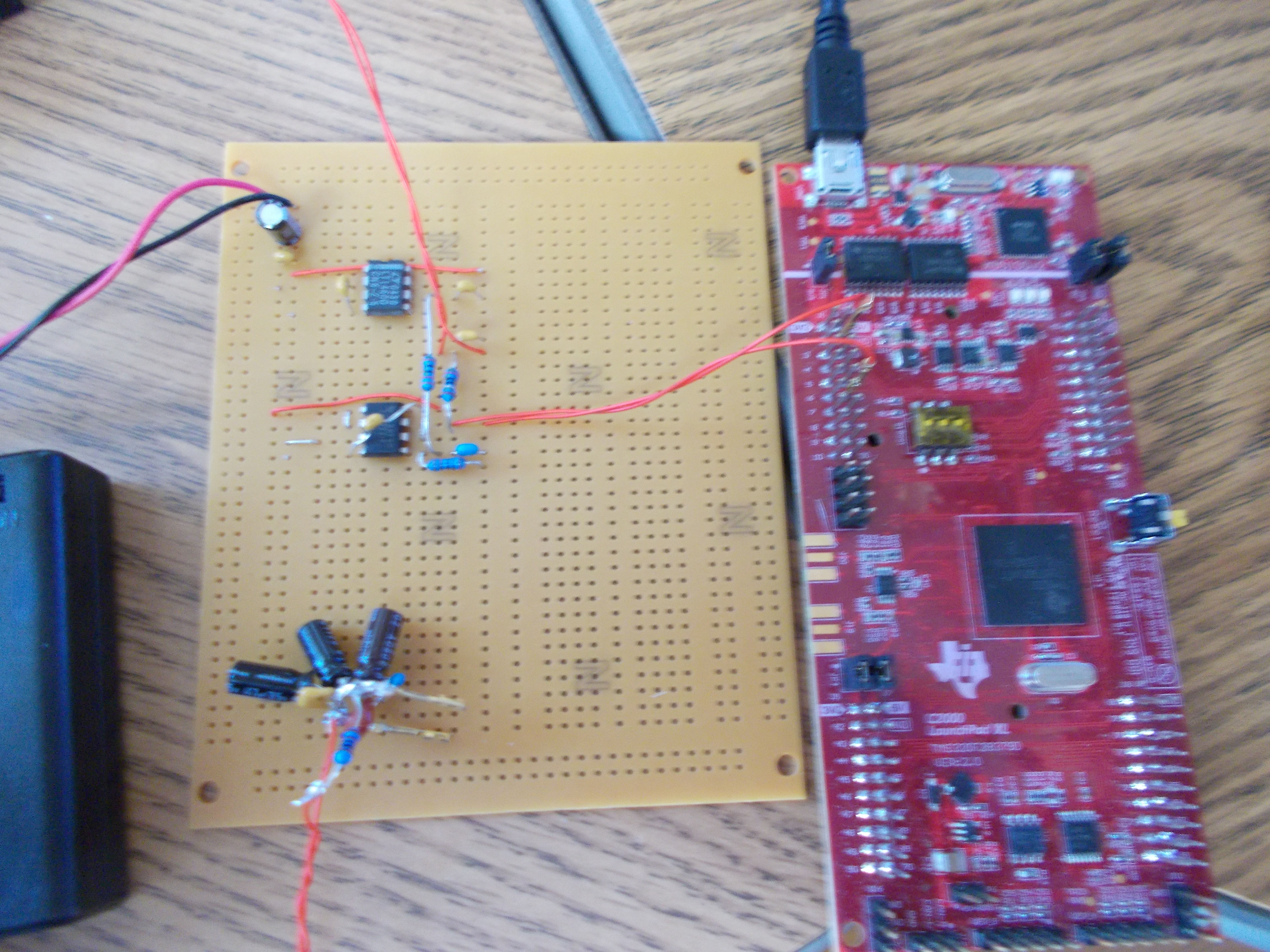
I have an application where we use a TMS320F28377D and the A/D channels are noisier than anticipated.I used channel A3. The A.D are setup as single ended 12 bit. In order to duplicate or create a contrast to leverage, I used a LaunchXL-F28379D. When this is shorted to gnd I only get one LSB of variation. Then when I apply 1.591 V (alkaline battery) with 0.1uF ceramic and 10 uF electrolytic in parallel, I get 7 or 8 LSB of variation. In the application using the TMS320F28377D the variation is consistently 12 LSB. i also changed the Sample/Hold count from 14 (75 nS) to 200 with no effect. If I am interpreting the specs correctly (SNA of 68.8) the noise should be around 2 LSB. So my first question is why does the LaunchXL have 7-8 LSB when the spec is around 2 LSB? Is there some grounding techniques I am missing, or are there special coding items I need to pay attention to? If I can get the LaunchXL to meet spec, then I am in better position to apply to the application. Any advice or material would be appreciated.

         Thanks!

  • Hi David,

    You are going to have some issues getting good performance from a battery, from anything with non-shielded floating wires, and from something that isn't buffered on the board.

    How about picking up something like this SMT boosterpack: http://store.43oh.com/index.php?route=product/product&product_id=69 or some regular protoboard plus SMT footprint adapters like so: https://www.mouser.com/ProductDetail/Texas-Instruments/DIP-ADAPTER-EVM?qs=T1E5mKGHTGV%2FfPkUlVRWNA%3D%3D&gclid=Cj0KCQjwybD0BRDyARIsACyS8mu0EdyG9c-l1NFiVs3SJzJBkjWDEuu2tWXfDuuiPeLQbvvM5uAXhusaAryVEALw_wcB

    And then building a nice ADC drive circuit along the lines of:

    In the top circuit you can get a nice clean DC voltage from a DC reference IC and then adjust the level as needed via the voltage divider.  

    In the bottom circuit you use a function generator to source in a good DC (or other signal like a sine wave) with a shielded SMA or BNC cable.

    In both cases, you'll want to ensure good ground return paths by running ground return wires adjacent to (or even twisted with) any wire routes on the protoboard.

    You can also play around with the component values.  20ohm + 330pF should allow very fast sampling with reasonably short S+H duration, but you can increase the RC here a little bit (maybe as high as say 60 ohm + 3.3nF) to get some more LP filtering at the expense of a longer S+H time.  

  • Thanks Devin,

    After some more testing with the same results, this was going to be my next step.  Some good info. However, the application using the TMS320F28379D pretty much has this circuit as the front end with even poorer results. Will keep you posted on how this turns out.

  • Devin,

    No matter what I do (including the circuit you provided), the best I can do on Chan A3 of the LaunchXL board is 7 or 8 LSB of peak to peak noise.

    My next steps are:

    Try some very simple code, maybe I've missed something.

    Try the diff amp circuit on the LAUNCHXL board

    Again, if there are some app notes you can suggest, I would be grateful.

       Thanks for your time.

  • Hi David,

    Can you send a picture of your physical setup?

    Also, what are you using as the input?  The buffer circuit can not remove noise if you source the voltage from a battery or some other unstable source.  You will want to use a reference IC or function generator.  

  • Devin,

    I used the circuit you provided, a reference voltage followed by an non inverting op amp. A battery was used as the voltage supply to the circuit to make sure there was no supply noise or common mode. I tried with the output RC in the circuit, then with the op amp directly to the Channel A3, and then through a large RC (1k and greater than 100uF with multiple ceramics to get the high freq impedance down)

        Thanks for your time

  • Hi David,

    A couple points:

    I don't think  the output voltage of the battery is stable (at the level the ADC can discriminate) even over short periods of time.  Trying to use a battery to evaluate the performance is a common problem.  I think you'll need to use a function generator or will want to use a higher voltage and then down-regulate that via a reference voltage generator IC (e.g. REF 3030).

    Are you using OPA320 specifically, or a different op-amp?  Other op-amps are obviously fine, but you do want something with high bandwidth (say >5MHz) and good noise performance. 

    The other op-amp related topic you need to look out for is op-amp stability.  OPA320 is great at driving captive loads, but if you put a large uF level capacitance on the output or directly on the input, it will still potentially oscillate or have issues settling.  You may want to simulate your op-amp in SPICE to ensure it is stable.  We don't typically try to do much filtering between the driving op-amp and the ADC input; the capacitor is just there to prevent the op-amp from having to slew and the R is just enough to keep the op-amp driver stable.  In addition to stability, the op-amp needs to settle the ADC input fast (within the allocated S+H time) so having too large of an R-C can slow this down to the point of causing issues.  That being said, I have seen increasing the C on the ADC input from say 220-330pF to maybe 1-2nF help with noise (but at the expense of needing to increase the S+H time).  

    If you want to add some low-pass or anti-aliasing filtering, you would usually need to add another active op-amp stage before the ADC drive stage. 

    Otherwise it seems like you've done a pretty good job constructing your circuit.  I think you still might see a little improvement moving to SMT components in a board that is mated with the launchpad (but I'd recommend you chase down the other items first). 

    One known limitation of the launchpad is that it does not have R-C footprints for the ADC input passives (the nominally 20ohm and 330pF components).  ideally you'd want to have these close to the pin.  Note that the ControlCard EVM platform does have these footprints.  


  • Thanks Devin,

    In these last tests, the only thing I used the 6V battery for was to supply the electronics that created the reference voltage (REF and OpAmp), this was to make sure there was no common mode.

    8 LSB out of 3.3 volts is around 6 mV, and in looking at the schematic for the LAUNCHXL, it appears there is no special effort to create an isolated common for the analog. So 6 mV of gnd noise is entirely feasible in my perspective.

        Dave

  • Hi Dave,

    How many samples are you taking to get the codespread? It is generally a little better to use standard deviation since this somewhat controls for number of samples taken.  

    Yes, certainly the Launchpad has made some trade-offs for the sake of low cost.

    The ControlCard EVM should have slightly better performance and it should be possible to do even better in your end-application board.  

  • Thanks Devin,

    I am just using a max and min function, the read rate is 40 kHz. The max and min go to their limits pretty quick (within the visual response of the debugger), so I'm guessing the effective sample size is something less than 40k.

    At this point we have abandoned this effort and are using some digital filtering. If we get to the point where we can redesign the hardware, we will certainly take a closer look at this.

        Thanks again for your time,

                Dave

  • Hi David,

    You might try looking at a histogram of the results in the future as this can tell you quite a bit more.

    If the distribution is wide, then you have some white noise in the signal (or ADC reference).

    If the distribution is narrow, but you have some outliers, there may be a rare edge/event that is coupling into the ADC infrequently.

    If the distribution is bi-modal, this usually indicates that a fast clock signal is causing some interference with the ADC.  

  • Some very good points Devin, thanks for the tip.

          Dave