This thread has been locked.

If you have a related question, please click the "Ask a related question" button in the top right corner. The newly created question will be automatically linked to this question.

TMS320F28377S: TMS320F28377SPTPT: About device Internal circuit architecture

Part Number: TMS320F28377S
Other Parts Discussed in Thread: LAUNCHXL-F28379D

Hi TI C2000 Expert,

We have a trouble on TMS320F28377SPTPT :

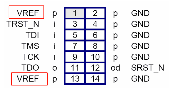
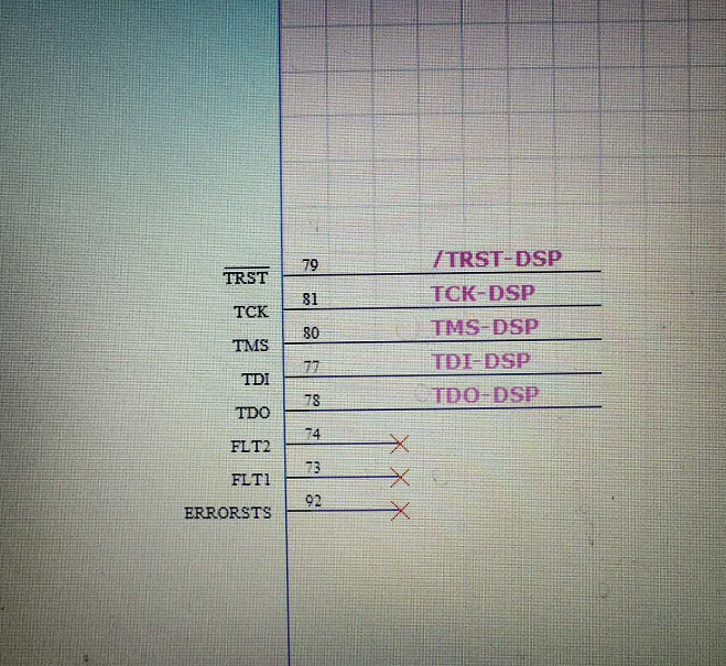
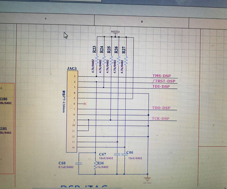
F28377 PCBA------14-pin TJAG------Emulator----usb--PC

Above is the Code burn path; Below is JTAG sche.

When we power on device with VDD3.3V, pin139(GPIO72) level status is uncertain, that will cause device enter boot mode if the level is low.

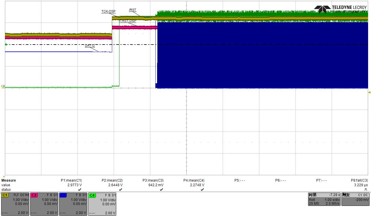
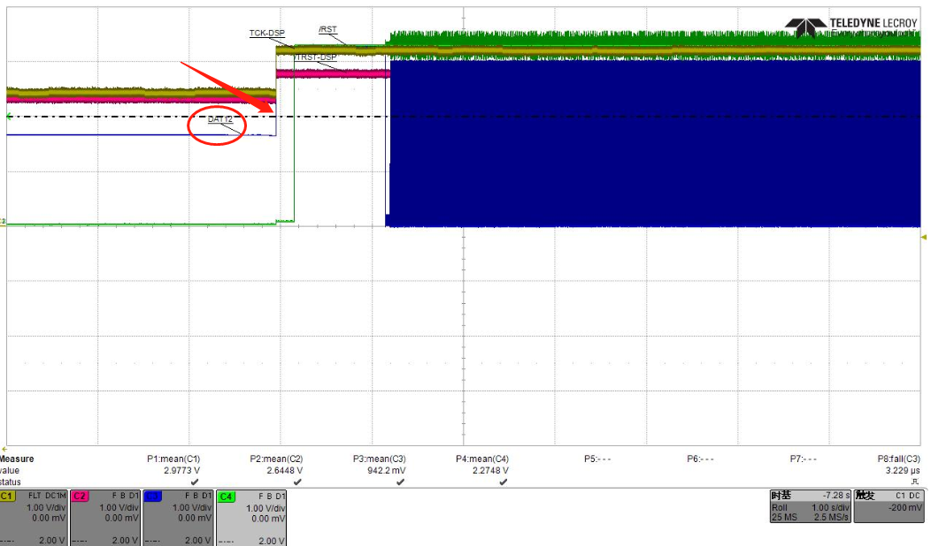
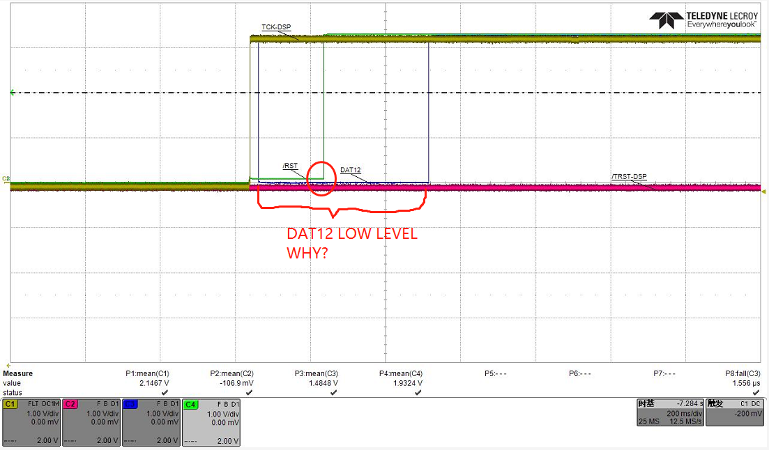
a. when the JTAG is unpluged in,  then powered on VDD3.3V, We can detect the wave on pin139/GPIO72/DAT12 as below image, when /RST is trigger, the DAT12 is low, it cause device enter boot mode, that's not we want.

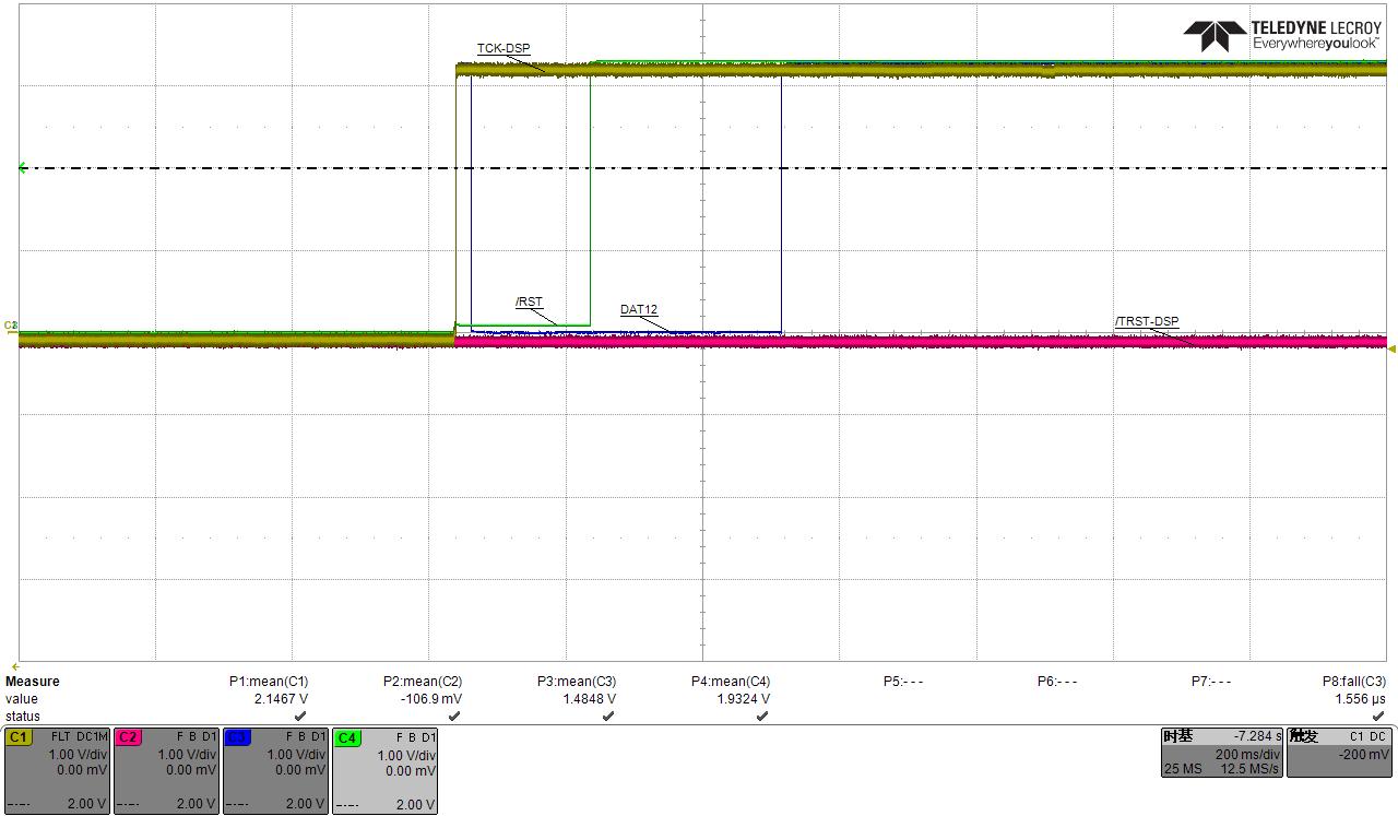
b. when the JTAG is pluged in,  then powered on VDD3.3V, We can detect the wave on pin139/GPIO72/DAT12 as below image,the question is:

    1. Do you know why there is an unnormal Voltage(about 1.5V)on VDD net and also on PIN139(Dat12); what is the Internal circuit architecture of this device between JTAG pin & GPIO72&VDD?

    2. How to cover this issue (we don't want the device enter boot mode after device RST.)

  • Hi,

    Are you using GPIO72 as one of the BOOTMODE pins? 

    How are you connecting GPIO72 on your board? Can you provide schematic for that?

    If you go through "Table 6-13. Device Boot Mode" in data manual you will see if the nTRST pin is held "low" device will enter the boot mode defined by the pin settings of GPIO72 and GPIO84. 

    Regards,

    Nirav

  • HI Nirav,

    First of all, thank you for your reply.

    Maybe I didn't make it clear enough, Let me add a few points as follows:

    1. What we want to confirm is why the level of GPIO72 pin increases from 1.5v to 3.3v (while JTAG is plugged in) when the board is powered on.

      Where does the 1.5V of  DAT12 pin(GPIO72) comes from?  from Emulator JTAG PIN?  what's the Internal circuit architecture of F28377SPTP?

       you can check waveform as below:

    2. On the basis of point 1, when the RST level gets higher, the GPIO72 we detected is at a high level and the BOOT mode is not triggered. This is the result we want, and we don't want to trigger the BOOT mode.

    3. But, if we unplug in the JTAG, while the board powered on, GPIO level from 0 V to 3.3 V.  there apears the unnormal wave of  DAT12(gpio72) for a while(arround 330ms), see below image; When powered on,  /RST from low to high, then detect GPIO72 level, it is low, then device enter boot mode, that's not we want. We have no operation on GPIO72, the low level continues for a while and it is appeared unfounded,  that is not the result of what we want, do you know why?

    4. In combination with point 2 and 3, may I ask how this difference is caused under two different operations(plug or unplug JTAG)? In addition, why does JTAG PIN cause 1.5V voltage of both GPIO72 PIN and VDD3.3 PIN? Do you know Why?

    5. In addition, we have tried to cut off the 3.3v power supply(JTAG vref) which is connected to PCBA,Still the GPIO and VDD3.3 were measured with a voltage of 1.5V. the Electric power is transmitted by PIN name of /TRST-DSP and TCK-DSP.

    Please help to confirm one by one, thank you.

  • Hi,

    Here are the answers to your questions in order:

    1. 1.5V on GPIO72 suggests that pin is floating, hence I asked for the schematic on this pin, are you connecting this pin to any special circuit, there should not be any voltage on this pin when the DSP is powered OFF. When the device powers up, PULL up gets enabled, and hence the GPIO72 goes from 1.5V to 3.3V.

    2. GPIO72 is a by default BOOTMODE pin, if you do not want to use this pin as BOOTMODE, you can configure some other pin, please refer to the BOOTMODE section in Data Sheet. 

    3. When JTAG is connected nTRST is high, hence GPIO72 will be dont care, and it will always boot up in Emulation mode. This is the reason when you connect JTAG you dont see this pin being used as boot mode pin and are able to observe desired waveforms. When you disconnect JTAG, nTRST is low, and hence it relies on this pin to determine the BOOTMODE

    4. I am suspecting some connection to this pin on Board, hence you see the 1.5V when the JTAG is connected before powering up the device. Please provide schematic of the routing on this pin.

    5. Can you also share the power routing on your board? Are you using the external Voltage regulator to power the device?

    Regards,

    Nirav

  • 2020041900001.pdf

    Attached schematic FYI.

    Please help to comfirm.

  • Hi Nirav,

    Could you please give us some advice according the schematic.

    Wait for it.

    Thanks.

  • How is VCC3.3 powered? Is it powered through external Regulator?

    I see GPIO72 and GPIO85 are pulled up via VCC3.3, why?

    If you are not connected to JTAG, how do you want to boot the device, which boot mode you want to use?

    As, I mentioned GPIO72 and GPIO84 are default boot mode pins, and based on your schematic GPIO72 is pulled High and GPIO84 has not external connection. Also I see you have pulled GPIO85 high? Are you trying to do SCI boot?

    Regards,

    Nirav

  • Hi Nirav

    Thank you very much for your patience and help,We still need your support.

    Here is the points for you.

    1.  V3.3 is obtained through the BUCK TPS562209DDCR.

    2.  JTAG is only used when downloading the DSP program and debugging, only to find that, even if the power has been cut off, JTAG also caused the DSP power pin and GPIO72 has 1.5V voltage. If you have EVM on hand, just try it. You can copy these phenomenon & waves using your EVM.

    3. Of course, we used the default BOOTLOAD startup mode, GPIO72 to pull up. If we used BOOT mode, we would manually handle GPIO84. However, what you answered is not what I want.

    4. My question is why GPIO72 is obviously pulled up and why there is occasionally low level when the reset signal is triggered. Here, I don't control GPIO72 at all.

  • Hi Nirav

     Due to this exception, our production line has been shut down, please expedite help to deal with it, thanks.

  • Hi,

    What signal is /RST? Is it same as XRSn?

    On the EVM at my end I dont see GPIO72 go low, it stays high.

    Based on your schematic, I see GPIO72 pulled up to VCC3.3V, but it is also connected to UART and FPGA, this may cause contention depending on the biasing of that pin on FPGA or UART. Is it possible to disconnect GPIO72 from UART and FPGA and then observe the similar waveform?

    Regards,

    Nirav

  • Hi Nirav,

    Can I understand it as you cannot get the same test result with EVM in lab? Power up with or withnot JTAG doesn't influence the GPIO72, right?

    Can you share with us the EVM number, how did you test it and also the waveform. thank you!

    Yuan

  • Yuan,

    We looked at this on the LAUNCHXL-F28379D launchpad http://dev.ti.com/tirex/explore/node?node=AH3P2nkmCQrJ0.EvACZ4ng__FUz-xrs__LATEST and didn't see an influence on GPIO72 from the JTAG being connected or not.

    I've read through the posts on this thread, and I'd like to make one correction.  Most internal Pull Ups(including the one on GPIO72) are disabled at reset, and all IOs are inputs.  We see that you have a 10k PU on GPIO72, but this pin is also going to the Microchip LAN IC as well as an EEPROM.  

    Would it be possible to dis-connect these ICs and see if the issue persists?  

    Also I wanted to make sure you also had pull on GPIO84 as it is also a default boot pin. I beleive you want both of these to be high to go into the GETMODE boot mode, correct?

    Best,

    Matthew